 机器人摄像头023ov5116n

《机器人摄像头023ov5116n》由会员分享,可在线阅读,更多相关《机器人摄像头023ov5116n(5页珍藏版)》请在装配图网上搜索。
1、OV5116NOV5116N SINGLE IC CMOS MONOCHROME CAMERA WITH NTSC ANALOG OUTPUTFeaturesnSingle chip 1/4 inch format video image sensornEIA/NTSC outputnSelectable mirror imagenAuto gain control (maximum + 18 dB)nHigh I.R. sensitivity for nighttime applicationsnAuto and manual backlight compensation modenGamm
2、a correction -On/OffGeneral DescriptionThe OV5116N is a complete black and white CMOS VideoCamera chip. It conforms to EIA/NTSC (60 Hz) standardsand outputs composite video capable of directly driving a 75display device. The on-chip auto exposure allows for a wide range of lightingconditions, elimin
3、ating the need for external mechanical shut-ter components. This, along with its single supply, low powerconsumption makes the OV5116N an incredibly versatile andcost-effective video camera perfect for the following types ofapplications:nExternal frame sync capabilityn40mw on-chip power consumptionn
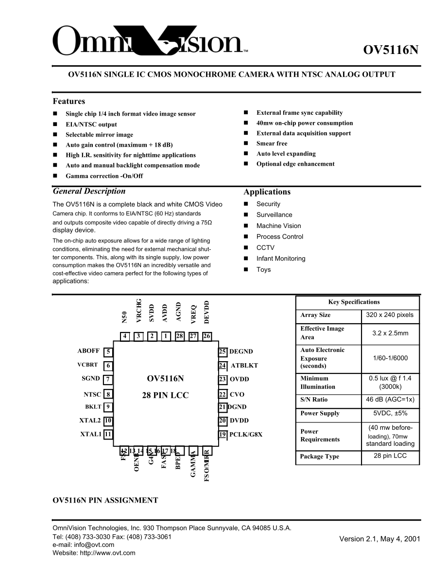
4、External data acquisition supportnSmear freenAuto level expandingnOptional edge enhancementApplicationsnSecuritynSurveillancenMachine VisionnProcess ControlnCCTVnInfant MonitoringnToysKey SpecificationsArray Size320 x 240 pixelsABOFFVCBRT56432128272625DEGND24ATBLKTEffective Image AreaAuto Electronic
5、 Exposure (seconds)3.2 x 2.5mm1/60-1/6000SGND7OV5116N23OVDDMinimum Illumination0.5 lux f 1.4(3000k)NTSC8BKLT9XTAL210XTAL11128 PIN LCC12 13 14 15 16 17 1822CVO21 DGND20DVDD19PCLK/G8XS/N RatioPower Supply PowerRequirementsPackage Type46 dB (AGC=1x)5VDC, 5%(40 mw before-loading), 70mw standard loading2
6、8 pin LCCOV5116N PIN ASSIGNMENTOmniVision Technologies, Inc. 930 Thompson Place Sunnyvale, CA 94085 U.S.A.Tel: (408) 733-3030 Fax: (408) 733-3061e-mail: infoWebsite: Version 2.1, May 4, 2001 SVDD AV D D N5 0 FS I DEVDD GAM M A AGND OENB FA S T BPED VRC H G VREQ G4X FS O /M IR ROMNIVISION TECHNOLOGIE
7、S, Inc.OV5116N1. IntroductionSINGLE IC CMOS MONOCHROME CAMERA WITH NTSC ANALOG OUTPUTThis section describes the features and functions of the OV5116N, a monochrome CMOS video camera integrated circuit.2.Pin Assignments:Table 1.Pin Descriptions Pin #1, 2, 20, 23, 2634567, 21, 25, 288*9101112131415161
8、7NameAVDD, SVDD,DVDD, OVDDDEVDDVRCHGN50ABOFFVCBRTSGND, DGND,DEGND, AGNDNTSCBKLTXTAL2XTAL1FSIOENBG4XFASTBPEDGAMMAClassBiasOAI-I-OABiasI-1I-XOXII-I-I-I-I-I-1Function Power (+5V) connections.Internal voltage reference. Connect to AGND with a 0.1uF capacitor. Set low()=standard NTSC. Set high (1)=50hz l
9、ight (For use in Japan Only);Auto brightness level descending function offVideo DC Output Black level, leave it open in usual caseGround connections. Connect to supply common.Set high(1)=EIA/NTSC modeBacklight mode 1Oscillator clock output or crystal output. External oscillator input or crystal inpu
10、t: 12.288MHzExternal frame sync input. A rising edge on FSI sets the chip timing to vertical sync. Leave open if unused.A logic level input to enable or tri-state CVO. Logic high(1)=tri-state;low()=enabled.A logic level input which when high places the maximum AGC gain to 4x. When low thesensor AGC
11、gain is 2x.A logic level input to enable/disable AGC/AEC FAST mode. High enables, low disables, which provides slow and smooth AGC/AEC mode.A logic level input to disable on chip edge enhancement. High disable, low enable.A logic level pin to select the transfer characteristic of output voltage vers
12、us light input. Logic high for g=0.45; low for g=1.18 FSO/MIRRI/O/In/out pin.Frame Sync Output. Digital frame sync output pin. Positive pulse occurs duringthe CVO vertical sync period. Input is a logic level input to enable mirror function. Low()=Standard, High(1)=Mirror.1922*2427PCLK/G8XCVOATBLKTVR
13、EQI/O/QI-OADigital pixel clock output. Provides 2 functions: When high a valid pixel is present at CVO and in sync with PCLK. Input is a logic level input to enable maximum AGC gain to 8x(only effective when pin 14 is set to high(1)The composite video output signal. The output is a source follower c
14、apable of directly driving a 1V p-p signal into a 108 load.(75 external and 33 internal)Backlight mode 2Internal voltage reference level. Connect to AGND with a 0.1uF capacitor.* Pin 9 and Pin 24 must be used in a logical combination as per the following table:ATB LK(Pin 24)BLK T(Pin 9)Mode11Class11
15、Default LevelNorm al ModeMode 1 - M anual B ack lightMode 2 A utom atic B ack light (Chip determ ination)Future UseI-1I-I/OOAQXI/XOBias: Low; O: OutputMay 4, 2001digital input, w ith 100k pull updigital input, w ith 100k pull dow ndigital C MOS level input and outputanalog C MOS reference voltage75
16、ohm outputcrystal input/outputpower supply biasVersion 2.12OMNIVISION TECHNOLOGIES, Inc.OV5116NSINGLE IC CMOS MONOCHROME CAMERA WITH NTSC ANALOG OUTPUT3. Electrical CharacteristicsTable 2. Electrical ParametersPARAMETERCONDITIONSMINTYPMAXUnitsVDDVpeakVblnkVsyncIDD1IDD2Cinfosctcyctr, tfPower supply v
17、oltageCVO output peak voltage*CVO output blank voltage*CVO output sync voltage*Functioning with 108 load on CVOFunctioning with 10k load on CVOMaximum pin capacitorCrystal/ceramic resonator frequency: 60HzPixel clock cycle time: 60HzMaximum digital input rise/fall time4.755.001.00.4012.2881635.25156
18、1020voltsvoltsvoltsvoltsmAmApFMHznsns* assuming standard loading of 108 (33 internal+75 external).Table 3. OV5116 TV Timing SpecificationParametersUnits1Number of lines per frame2Field frequency3Line period4Line blanking interval5Line synchronizing pulse6Field blanking interval 7First equalizing pul
19、se width8Field synchronizing pulse width 9Second equalizing pulse width 10FSO widthMay 4, 200152560.0163.47611.414.5622/233/2.532.5/33Version 2.1linesHzsecsecseclinelinelinelineline3OMNIVISION TECHNOLOGIES, Inc.OV5116N0.0020.0030.0600.006SINGLE IC CMOS MONOCHROME CAMERA WITH NTSC ANALOG OUTPUTNOTES:
20、1)All dimensions in inches.Bottom ViewTop View0.0200.0022 PA0.020 0.0020.0200.002A-A4150.050PIN 1INDEX0.3300.075 0.010111290.450 SQ. 0.0080.350 SQ. 0.0060.007 MAX.B/F PULL BACK0.011 MIN.870.010.x45PIN NO. 1INDEX610.013 MAX.B/F EXPOSURE2826250.0850.025 0.003 28 PLCSR 0.00928 PLCS0.035 MIN.19180.015 M
21、IN.4 PLCSR 0.0124 PLCS20210.200 0.00522230.0404 PLCS0.010 DIE1Scan Origin(Row #1, Column #1)Package Center(0, 0)Array Center(-0.011, -0.011)Scan End(Final Row, Final Column)SensorArrayTop ViewMay 4, 2001Note: Most lens assemblies reverse the viewed scene onto the sensor array,which generally means t
22、hat pin 1 should be located at the bottom of the p.c. board.To ensure correct display orientation, check the lens specification prior tolaying out the printed circuit board.Figure 1. OV5116 Series Package and Sensor Array DimensionsVersion 2.14 0. 050 0. 008 27 PL CS 0. 040 REF .x45 3 PL CS 0. 020 R
23、EF .x45 0. 024 22 P L C S 0. 014 24 P L C S 0. 300 S Q . 0 .0 05OMNIVISION TECHNOLOGIES, Inc.OV5116NSINGLE IC CMOS MONOCHROME CAMERA WITH NTSC ANALOG OUTPUTOV5116 Module Reference Design (Use for all new designs)J11PWR3U1MC78L05ACPVINVOUT1VCC(5V)CON1J21GNDC1.1U-0603C247U-16R1VCCVCCC3VCCJ4CON110K-060
24、3VCCR21U/TE-A10K-0603C4C5CON1GNDJ31CON1VCCR3R4.1U-0603.1U-0603U2VCCY1:13.5MHz, R9-on 50Hz, 352x288R810K-060310K-060310K-060356ABOFF7VRBRT25DEGND24ATBLT23R5R6R7J5NTSC8SGNDOVDD22CVOY1:12.288MHz, R9-off 60Hz, 320x24019NTSCOV5116CVO21CON110BKLTDGND20J6R8 R5OFF OFF NormalON OFF Manual Back LightOFF ON Au
25、to Back Light1ON ON Auto Back Light2R15 4x max gainR14 AGC/AEC Fast mode (10k pull up resistor for outdoor use)R910K-0603J8CON1Y1X-12.288MR1111XTAL2XTAL1DVDDPCLK/G8X19G8XMIRRJ7CON1R101CON1VCCJ10R12 Bypass EdgeR13 Gamma offC61M-0603C7J91CON1FSIOENBR12GAMMAVCC10K-0603R131CON1R10 Mirror modeR7 8X GAIN(
26、Effect only R15on)R2 N50 modeR4 Auto Brightness OffR9 Pal/Ntsc SwitchR1/R3 Adjust Brightness level(open at normal case)Option10P-060310P-0603J111CON110K-0603R1410K-0603FASTG4XJ121CON1R1510K-0603J131CON110K-0603TitleOV5116MD930 Thompson Place, Sunnyvale, CA 94086Phone 408-733-3030 Fax 408-733-3061Siz
27、eDocument NumberRevCustomOV5116 MODULESADate:Tuesday, September 21, 199911Figure 3. Reference Design for OV5116 (Use for all new designs)OmniVision Technologies, Inc. reserves the right to make changes without further notice to any product herein to improve reliability, function, ordesign. OmniVisio
28、n Technologies, Inc. does not assume any liability arising out of the application or use of any product or circuit describedherein; neither does it convey any license under its patent rights nor the rights of others. No part of this publication may be copied or repro-duced, in any form without the prior written consent of OmniVision Technologies, Inc.May 4, 2001Version 2.15 10K-0603 2 GND 10K-0603 1 33-0603 17 12 13 14 15 16 18 26 27 28 1 2 3 4 GAMMA FSI OENB G4X FAST BPED FSO/MIRR DEVDD VREQ AGND AVDD SVDD VRCHG N50 1 1
- 温馨提示:
1: 本站所有资源如无特殊说明,都需要本地电脑安装OFFICE2007和PDF阅读器。图纸软件为CAD,CAXA,PROE,UG,SolidWorks等.压缩文件请下载最新的WinRAR软件解压。
2: 本站的文档不包含任何第三方提供的附件图纸等,如果需要附件,请联系上传者。文件的所有权益归上传用户所有。
3.本站RAR压缩包中若带图纸,网页内容里面会有图纸预览,若没有图纸预览就没有图纸。
4. 未经权益所有人同意不得将文件中的内容挪作商业或盈利用途。
5. 装配图网仅提供信息存储空间,仅对用户上传内容的表现方式做保护处理,对用户上传分享的文档内容本身不做任何修改或编辑,并不能对任何下载内容负责。
6. 下载文件中如有侵权或不适当内容,请与我们联系,我们立即纠正。
7. 本站不保证下载资源的准确性、安全性和完整性, 同时也不承担用户因使用这些下载资源对自己和他人造成任何形式的伤害或损失。
最新文档
- 2020年春季部编版五年级下册第二单元8红楼春趣ppt课件
- 第三章-合理烹饪ppt课件
- 第三章-建筑施工测量ppt课件
- 第一章社区护理学ppt课件
- 部编版四年级下册语文第六单元习作:我学会了---------ppt课件
- 第三章--等参数单元(等参元)ppt课件
- 2020学年【苏科版】数学七年级上册:3.1《字母表示数》ppt课件
- 【课件一】711有序数对
- 2019高后果区识别ppt课件
- 一二节餐饮礼仪课件
- 第三章---土地利用规划体系ppt课件
- 2019版人教版七年级生物教材与实验教材对比分析ppt课件
- 2020年大气污染及防治新ppt课件
- 第三章-客户生命周期及价值ppt课件
- 2020年大气污染主要来源ppt课件
