 USB2.0标准保护电路设计指南图文精

《USB2.0标准保护电路设计指南图文精》由会员分享,可在线阅读,更多相关《USB2.0标准保护电路设计指南图文精(5页珍藏版)》请在装配图网上搜索。
1、st tDnatu?2*lnis tE98ffnd&nf CBtoto-2 MMm-DaBeMVV ilf ium-n?i * * if iff maYtww-“s jf1“l“ I l9QBtBW3R Ous asa ?! t r-t i It-fur? a n fa $t. fn n I vv m If fssAf Its atl a 9ZEm曲口Mv vwm? a LtaH TPJw i!wK flu pm ip y 4w gr熠dri w nwfliMH. W jMM.cm iW RMn li * I-VHrf !* -耳 IM-LjHWH MOif* 枪E M-碎 * EWM VI
2、AMLBLi Vv4 tBD telQ vW mR * * Wdq nnHUB-A*PB4 rHrihp 4ww W twmniFBfB 他 dmAh ph*H hh 4m ihAh krr b4amr tar mAht d uw inKkoi tart yau-cmat MnaB ita A*m EtvvBqgwdtq JM fcf Iw arifr. W Mt MMaMrwtaAiU FI1a aMlA*M p*-?亍M*q tn*V RW- ! if-FT- d rB *1 WV T.r-HMBf ,、 F F“ Mftl 0 BmJ to V accnto! d. biJMiwM af
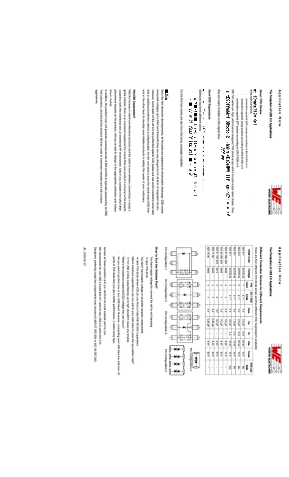
3、cHMwtfw* n 皿-rMUC* * iKH MwiMW4*?! taEw*hF WO KI abni *few Vvrm f jfu Vv 4hW*TVv wfcluu tlNtai Mfl -ImmW! Ita nMMf 律 jnJ frm MoAmf vvI.bM. 2 靖 *X fi;ih4Tw_el iniM a-Application Note The Protection of USB 2.0 Applicatio ns Order Code 824 015 Competitor S 824 001 Competitor P I/O VRWM VCI,IO VCI,VDD V
4、ESD CIN IPP Package SOT23-6L SOT23-6L SOT23-6L SOT23-6L I/O 4 4 4 4 VRWM 5 5 5 5 V CI,IO 12 22 14 28 VCI,VDD 7,5 15,5 9 19 VESD 12 kV 15 kV 8 kV 8 kV C IN 2 pF 3 pF 1 pF 3 pF IPP 12 A 12 A 5A 6A Number of I/O lines the TVS-Diode can protect Max. reverse worki ng voltage ESD clampi ng voltage at I/O
5、pin (IEC 61000-4-2, con tact mode at 6kV ESD clampi ng voltage at VDD pin (IEC 61000-4-2, con tact mode at 6kV Max. withsta nding ESD pulse (IEC 61000-4-2, con tact mode In put capacita nee at I/O pin via. GND (VIN = 2,5 V, VDD=5V Max. Withsta ndi ng surge curre nt (8/20 s TLP Curve of differe nt pa
6、rts for VDD TLP Curve of differe nt parts for I/O lines Recomme nded Layout for Si ngle Sin gle USB Port The two differe ntial sig nal li nes (D+ and D- are routed from conn ector to TVS-Diode (p/n 824 011 and via a com mon mode choke (p/n 744 232 090 to the USB con troller as show n on the left pic
7、ture below. This results in an awesome ESD protect ion and EMI suppressi on of both data lin es. VBUS is routed like the sig nal line, but in stead of the com mon mode choke a chip bead ferrite (p/n 742 792 641 is used.After the chip bead you may add a capacitor and a sec ond chip bead as well to ge
8、t the highest possible EMI suppression effect. For very sensible IC s and / or high reliableapplicati ons you can get an optimized ESD suppressi on effect if you double con tact a four-fold TVS array (p/n 824 015 like shown on right picture. JB, 2009-06-23 Page 6 of 9Application Note The Protection
9、of USB 2.0 Applicatio ns Protection of si ngle USBport Double protecti on of sin gle USB port Desig ners preferri ng sin gle cha nnel comp onents can also use the ESD Suppressors WE-VE. The conn ecti on has to be carried out from D+ / D- to GND. The other parts are connected in same way as above.Pro
10、tectio n of si ngle USB port Recomme nded Layout for Double USB Port Accordi ng to sin gle USB port protect ion the routi ng is very similar. Use here exactly the same parts as for single port protection and the protection level will also be the same. Protection of double USB port JB, 2009-06-23 Pag
11、e 7 of 9Application Note The Protection of USB 2.0 Applications Bill of Material: Material:In this application note the following parts are used TVS-Diodes WE-TVS: 824 011: 824015: Protection of 2 I&O lines and VDD line: Size SOT23-5L | 2pF CI/O | 5V VRWM | 5A IPP Protectio n of 4 I&O lines and VDD
12、line: Size SOT23-6L | 2pF CI/O | 5V VRWM | 5A IPP ESD Suppressors WE-VE: 823 07 050 029: 823 06 050 029: Size 0402 | 0.2pF Ctyp | 5V VRWM | 17V VCL Size 0603 | 0.2pF Ctyp | 5V VRWM | 30V VCL Com mon Mode Chokes WE-CNSW: 744 232 090: Size 1206 | 370mA IDC | 300 m? RDC | 90?Impeda nee Chip Bead Ferrit
13、es WE-CBF: 742 792 641: Size 0603 | 2 000mA IDC | 150 m? RDC | 300? Impedanee USB-Connectors WR-COM: 614 008 260 21: 614 004 135 023: USB Typ A Co nn ector | THT | Dual stacked USB Typ A Co nn ector | THT | Vertical JB, 2009-06-23 Page 8 of 9Applicati on Note The Protectio n of USB 2.0 Applicati ons
14、 In terface Desig n Kit For an easy desig n of in terfaces Wrth Elektr onik has laun ched a special In terface Desig n Kit. This desig n kit in cludes a desig n guide for USB 1.0 to USB 2.0, CAN, Ethernet, VGA, DVI, RS232 and RS485 in terfaces and all the compo nents used. These are ESDSuppressors,
15、SMD Common Mode Chokes, Chip Bead Ferrites, LAN Tran sformers and the corresp onding Conn ectors. In total are 35 differe nt passive comp onents with 235 parts and 4 evaluations boards in. The colour scheme makes it easy to locate the suitable parts for your application. Just follow the specific application colour and arrange your needed parts. For each application you find a simple block schematic where you see how to place the different components to get the best result. Try it it s worth each penny pen ny! ny ! JB, 2009-06-23 Page 9 of 9
- 温馨提示:
1: 本站所有资源如无特殊说明,都需要本地电脑安装OFFICE2007和PDF阅读器。图纸软件为CAD,CAXA,PROE,UG,SolidWorks等.压缩文件请下载最新的WinRAR软件解压。
2: 本站的文档不包含任何第三方提供的附件图纸等,如果需要附件,请联系上传者。文件的所有权益归上传用户所有。
3.本站RAR压缩包中若带图纸,网页内容里面会有图纸预览,若没有图纸预览就没有图纸。
4. 未经权益所有人同意不得将文件中的内容挪作商业或盈利用途。
5. 装配图网仅提供信息存储空间,仅对用户上传内容的表现方式做保护处理,对用户上传分享的文档内容本身不做任何修改或编辑,并不能对任何下载内容负责。
6. 下载文件中如有侵权或不适当内容,请与我们联系,我们立即纠正。
7. 本站不保证下载资源的准确性、安全性和完整性, 同时也不承担用户因使用这些下载资源对自己和他人造成任何形式的伤害或损失。
