 半导体工艺学silvaco仿真实例——扩散

《半导体工艺学silvaco仿真实例——扩散》由会员分享,可在线阅读,更多相关《半导体工艺学silvaco仿真实例——扩散(8页珍藏版)》请在装配图网上搜索。
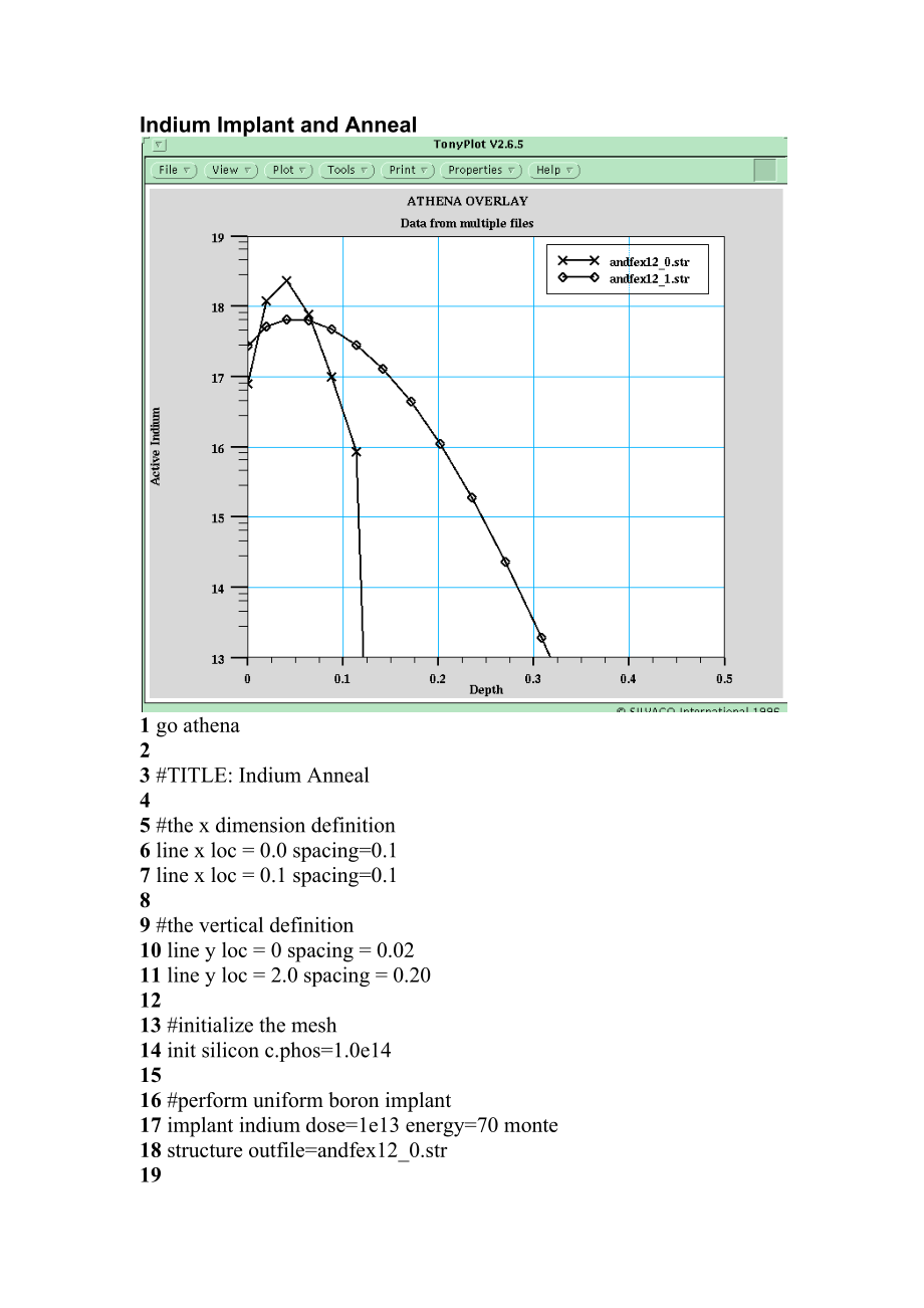
1、Indium Implant and Anneal1 go athena23 #TITLE: Indium Anneal45 #the x dimension definition6 line x loc = 0.0 spacing=0.17 line x loc = 0.1 spacing=0.189 #the vertical definition10 line y loc = 0 spacing = 0.0211 line y loc = 2.0 spacing = 0.201213 #initialize the mesh14 init silicon c.phos=1.0e14151
2、6 #perform uniform boron implant17 implant indium dose=1e13 energy=70 monte18 structure outfile=andfex12_0.str1920 #perform diffusion21 diffuse time=30 temperature=1000222324 extract name=xj xj silicon mat.occno=1 x.val=0.0 junc.occno=12526 #save the structure27 structure outfile=andfex12_1.str2829
3、tonyplot -overlay andfex12_0.str andfex12_1.str -set andfex12.set3031 quitOxidation Enhanced Diffusion of Boron1 go athena23 # OED of Boron45 #the x dimension definition6 line x loc = 0.0 spacing=0.17 line x loc = 0.1 spacing=0.189 #the vertical definition10 line y loc = 0 spacing = 0.0211 line y lo
4、c = 2.0 spacing = 0.2012 line y loc = 25.0 spacing = 2.51314 #initialize the mesh15 init silicon c.boron=1.0e141617 #perform uniform boron implant18 implant boron dose=1e13 energy=701920 #set diffusion model for OED21 method two.dim2223 #perform diffusion24 diffuse time=30 temperature=1000 dryo225 #
5、26 extract name=xj_two.dim xj silicon mat.occno=1 x.val=0.0 junc.occno=12728 #save the structure29 structure outfile=andfex02_0.str3031 # repeat the simulation with default FERMI model32 go athena3334 #TITLE: Simple Boron Anneal3536 #the x dimension definition37 line x loc = 0.0 spacing=0.138 line x
6、 loc = 0.1 spacing=0.13940 #the vertical definition41 line y loc = 0 spacing = 0.0242 line y loc = 2.0 spacing = 0.2043 line y loc = 25.0 spacing = 2.54445 #initialize the mesh46 init silicon c.phos=1.0e144748 #perform uniform boron implant49 implant boron dose=1e13 energy=705051 #select diffusion m
7、odel52 method fermi5354 #perform diffusion55 diffuse time=30 temperature=1000 dryo256 #57 extract name=xj_fermi xj silicon mat.occno=1 x.val=0.0 junc.occno=1585960 #save the structure61 structure outfile=andfex02_1.str6263 # compare diffusion models64 tonyplot -overlay andfex02_0.str andfex02_1.str
8、-set andfex02.setEmitter Push Effect1 go athena23 #TITLE: Emitter push effect example4 #5 line x loc=0.0 spac=0.26 line x loc=2.5 spac=0.87 line x loc=3.0 spac=0.28 #9 line y loc=0.00 spac=0.0410 line y loc=0.3 spac=0.0611 line y loc=2.0 spac=0.812 line y loc=10.0 spac=2.013 #14 init c.phos=1e1515 #
9、16 implant boron dose=1e13 energy=4017 #18 deposit nitride thick=.2 div=419 #20 etch right nitride p1.x=2.521 relax y.min=1.522 #23 implant phosphor dose=1e16 energy=3024 #25 etch nitride all26 #27 method compress full.cpl28 diffuse time=30 temp=100029 #30 structure outfile=andfex07.str31 #32 tonypl
10、ot -st andfex07.str -set andfex07.set3334 quitDamage Enhanced Diffusion of ArsenicThis example demonstrates the damage enhanced diffusion effect in a heavy arsenic implant typicalof MOS source/drain or bipolar emitter processing.1 go athena23 #the x dimension definition4 line x loc = 0.0 spacing=0.1
11、5 line x loc = 0.1 spacing=0.167 #the vertical definition8 line y loc = 0 spacing = 0.0059 line y loc = 2.0 spacing = 0.2010 line y loc = 25.0 spacing = 2.51112 #initialize the mesh13 init silicon c.boron=1.0e171415 #deposit screen oxide16 deposit oxide thickness=0.005 div=21718 #perform arsenic imp
12、lant with damage19 implant arsenic dose=1.0e15 energy=40 tilt=7 unit.damage dam.factor=0.12021 #set diffusion model for TED22 method full.cpl2324 #perform diffusion25 diffuse time=15/60 temperature=100026 #27 extract name=xj_fullcpl xj silicon mat.occno=1 x.val=0.0 junc.occno=12829 #save the structu
13、re30 structure outfile=andfex03_0.str3132 # repeat the simulation with FERMI model3334 #the x dimension definition35 line x loc = 0.0 spacing=0.136 line x loc = 0.1 spacing=0.13738 #the vertical definition39 line y loc = 0 spacing = 0.00540 line y loc = 2.0 spacing = 0.2041 line y loc = 25.0 spacing
14、 = 2.54243 #initialize the mesh44 init silicon c.boron=1.0e174546 #deposit screen oxide47 deposit oxide thickness=0.005 div=24849 #perform arsenic implant with damage50 implant arsenic dose=1.0e15 energy=40 tilt=7 unit.damage dam.factor=0.15152 #set default model53 method fermi5455 #perform diffusion56 diffuse time=15/60 temperature=100057 #58 extract name=xj_fermi xj silicon mat.occno=1 x.val=0.0 junc.occno=15960 #save the structure61 structure outfile=andfex03_1.str6263 # compare diffusion models64 tonyplot -overlay andfex03_0.str andfex03_1.str -set andfex03.set
- 温馨提示:
1: 本站所有资源如无特殊说明,都需要本地电脑安装OFFICE2007和PDF阅读器。图纸软件为CAD,CAXA,PROE,UG,SolidWorks等.压缩文件请下载最新的WinRAR软件解压。
2: 本站的文档不包含任何第三方提供的附件图纸等,如果需要附件,请联系上传者。文件的所有权益归上传用户所有。
3.本站RAR压缩包中若带图纸,网页内容里面会有图纸预览,若没有图纸预览就没有图纸。
4. 未经权益所有人同意不得将文件中的内容挪作商业或盈利用途。
5. 装配图网仅提供信息存储空间,仅对用户上传内容的表现方式做保护处理,对用户上传分享的文档内容本身不做任何修改或编辑,并不能对任何下载内容负责。
6. 下载文件中如有侵权或不适当内容,请与我们联系,我们立即纠正。
7. 本站不保证下载资源的准确性、安全性和完整性, 同时也不承担用户因使用这些下载资源对自己和他人造成任何形式的伤害或损失。
