 AUO KD101N2-40NA-A1国显101寸TFT规格书

《AUO KD101N2-40NA-A1国显101寸TFT规格书》由会员分享,可在线阅读,更多相关《AUO KD101N2-40NA-A1国显101寸TFT规格书(18页珍藏版)》请在装配图网上搜索。
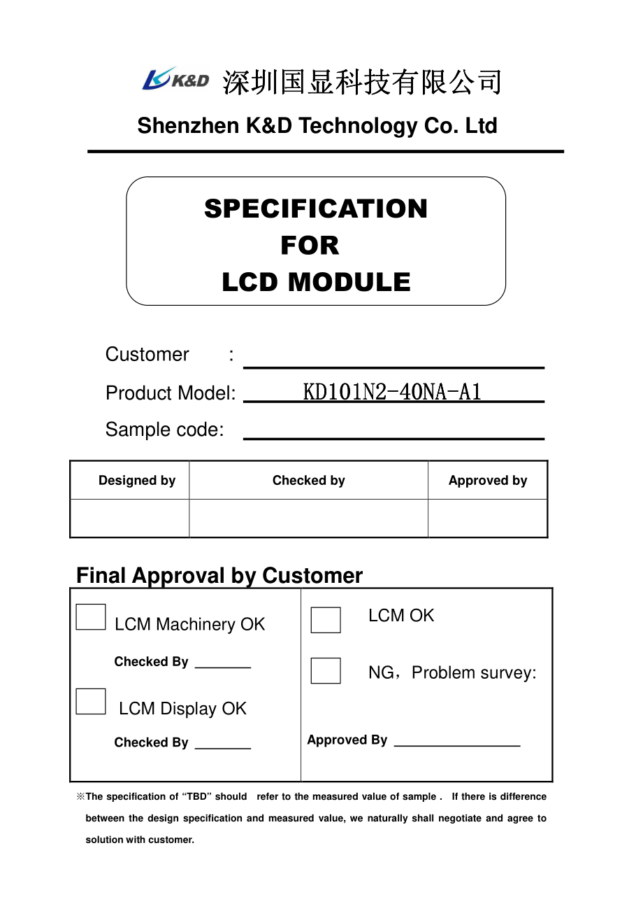
1、 深圳国显科技有限公司深圳国显科技有限公司深圳国显科技有限公司深圳国显科技有限公司 Shenzhen K&D Technology Co.Ltd SPECIFICATION FOR LCD MODULE Customer :Product Model:KDKDKDKD101N101N101N101N2 2 2 2-4 4 4 40 0 0 0N N N NA A A A-A A A A1 1 1 1 Designed by Checked by Approved by Final Approval by Customer LCM Machinery OK Checked By LCM Disp
2、lay OK Checked By LCM OK NG,Problem survey:Approved By The specification of“TBD”should refer to the measured value of sample.If there is difference between the design specification and measured value,we naturally shall negotiate and agree to solution with customer.Sample code:深圳国显科技有限公司 KDKDKDKD101N
3、101N101N101N2 2 2 2-4 4 4 40 0 0 0N N N NA A A A-A A A A1 1 1 1 All Rights Reserved 2/18 REV.A Revision History Version Contents Date Note A Original 2011.2.16 深圳国显科技有限公司 KDKDKDKD101N101N101N101N2 2 2 2-4 4 4 40 0 0 0N N N NA A A A-A A A A1 1 1 1 All Rights Reserved 3/18 REV.A Contents No.Item Page
4、1.Numbering System 4/18 2 Scope 5/18 3 Normative Reference 5/18 4 Definitions 5/18 5 Block Diagram 7/18 6 Technology Specifications 7/18 7 Reliability Test Condition and Methods 15/18 8 Handling Precautions 15/18 9 Precaution for use 17/18 10 Package Drawing 17/18 11 Outline Dimension 18/18 深圳国显科技有限
5、公司 KDKDKDKD101N101N101N101N2 2 2 2-4 4 4 40 0 0 0N N N NA A A A-A A A A1 1 1 1 All Rights Reserved 4/18 REV.A 1.Numbering System (1)(2)(3)(4)(5)(6)(7)(8)No Definition Specifications (1)TFT LCM Productor No.KD-King Display Technology Co.Ltd (2)Display monitor opposite angle line size Unit:mm or mmm(s
6、ize=10 inch:takes three integers)(3)Productor Types D-Digital photo frame/DVD G-GPS M-MP P-Mobil-Phone N-Net Book。(4)Productor Development Series No.By two figures characters expression from 01 to 99 (5)Interface PIN Number By two figures characters expression from 01 to 99 (6)With Touch Panel Or No
7、t T-With T/P;N-Without T/P (7)LCD Type A-AUO;M-CMO;C-CPT;P-PVI;L-LG;W-Wintek;H-HSD;T-Topply;Y-Hydis;I-Hitach;S-Sharp。(8)Productor Development edition No.By The English litters:A 1 Z9 深圳国显科技有限公司 KDKDKDKD101N101N101N101N2 2 2 2-4 4 4 40 0 0 0N N N NA A A A-A A A A1 1 1 1 All Rights Reserved 5/18 REV.A
8、 2.Scope This specification applies to the TFT LCD module which is designed and manufactured by LCM Factory of Shenzhen K&D Technology Co.Ltd.3.Normative Reference GB/T4619-1996 Liquid Crystal Display Test Method GB/T2424 Basic environmental Testing Procedures for Electric and Electronic Products.GB
9、/T2423 Basic Testing Procedures for Electric and Electronic Products IEC61747-1 SIXTH PARTGB28282829-87National Standard of PRC 4.Definitions 4.1 Definitions of Vop The definitions of threshold voltage Vth1,Vth2 the following typical waveforms are applied on liquid crystal by the method of equalized
10、 voltage for each duty and bias.【selected waveform】【non-selected waveform】Vth1:The voltage which the brightness of segment indicates 50%of saturated value on the conditions of selected waveform (ff=80Hz,=10=270at 25)Vth2:The voltage which the brightness of segment indicates 50%of saturated value on
11、the conditions of non-selected waveform (ff=80Hz,=10=270at 25)Vop:(Vth1(50%)+Vth2(50%)/2 (ff=80Hz,=10=270at 25)4.2 Definition of Response Time Tr,Td Tr:The time required which the brightness of segment becomes 10%from 100%when waveform is switched to selected one from non-selected one.(ff=80Hz,=10=2
12、70 at 25)Td:The time required which the brightness of segment becomes 90%from 10%when waveform is switched to selected one from selected one.(ff=80Hz,=10=270 at 25)深圳国显科技有限公司 KDKDKDKD101N101N101N101N2 2 2 2-4 4 4 40 0 0 0N N N NA A A A-A A A A1 1 1 1 All Rights Reserved 6/18 REV.A 4.3 Definition of
13、Contrast Ratio Cr Cr=A/B A:Segments brightness in case of non-selected waveform B:Segments brightness in case of selected waveform 4.4 Definition of Angle and Viewing Range Angular Graph:Constrast Ratio Such as:Viewing Angle Range:80(Cr2)Horizontal 70(Cr2)Vertical 深圳国显科技有限公司 KDKDKDKD101N101N101N101N
14、2 2 2 2-4 4 4 40 0 0 0N N N NA A A A-A A A A1 1 1 1 All Rights Reserved 7/18 REV.A 5.Block Diagram 6.Technology Specifications 6.1 Features This single-display module is suitable for use in Net Book products.The LCD adopts one backlight with High brightness 24-lamps white LED.Construction:10.1-Si co
15、lor TFT-LCD,White LED backlight,FPC and T-CON.6.2 General Specifications No.Item Specification 1 LCD size 10.1 inch 2 Resolution 1024(RGB)X600 3 Display mode Normally white,Transmissive 4 Pixel pitch 0.2175(W)X0.2088(H)mm 5 Active area 222.72(W)X125.28(H)mm 6 Module size 235.0(W)X143.0(H)X5.2(max)(D
16、)mm 7 Pixel arrangement RGB-stripe 8 Interface Digital(6bit LVDS)9 Backlight power consumption 2.500W(Typ.)10 Panel power consumption 0.26W(Typ.)11 Weight TBD 深圳国显科技有限公司 KDKDKDKD101N101N101N101N2 2 2 2-4 4 4 40 0 0 0N N N NA A A A-A A A A1 1 1 1 All Rights Reserved 8/18 REV.A 6.3 Interface Pin Conne
17、ction Connector CN1 is used for electronics interface.The recommended model is IPEX-20455-040E-12 manufactured by IPEX.Pin No.Symbol Function 1 NC No Connection(Reserve)2 VDD Power Supply,3.3V(typical)3 VDD Power Supply,3.3V(typical)4 V_EDID EDID 3.3V power 5 NC No Connection(Reserve)6 CLK_EDID EDID
18、 Clock 7 DATA_EDID EDID Data 8 Rin0-LVDS differential data input(R0-R5,G0)9 Rin0+LVDS differential data input(R0-R5,G0)10 GND Ground 11 Rin1-LVDS differential data input(G1-G5,B0-B1)12 Rin1+LVDS differential data input(G1-G5,B0-B1)13 GND Ground 14 Rin2-LVDS differential data input(B2-B5,HS,VS,DE)15
19、Rin2+LVDS differential data input(B2-B5,HS,VS,DE)16 GND Ground 17 ClkIN-LVDS differential clock input 18 ClkIN+LVDS differential clock input 19 GND Ground 20 NC No Connection(Reserve)21 NC No Connection(Reserve)22 GND Ground 23 NC No Connection(Reserve)24 NC No Connection(Reserve)25 GND Ground 26 NC
20、 No Connection(Reserve)27 NC No Connection(Reserve)28 GND Ground 29 NC No Connection(Reserve)30 NC No Connection(Reserve)31 GND Ground 32 GND Ground 33 GND Ground 34 NC No Connection(Reserve)35 PWM LED BLU Brightness Control(Note 1,2)36 LED-EN/NC LED Converter Enable(3.3V)/NC 37 NC No Connection(Res
21、erve)38 VLED LED Converter Input Power(5V21V)39 VLED LED Converter Input Power(5V21V)40 VLED LED Converter Input Power(5V21V)深圳国显科技有限公司 KDKDKDKD101N101N101N101N2 2 2 2-4 4 4 40 0 0 0N N N NA A A A-A A A A1 1 1 1 All Rights Reserved 9/18 REV.A Note1:PWM is used to adjust the B/Lbrightness.Note 2:PWM
22、signal=03.3V,Operation Frequency:100 Hz20KHz,6.4 Absolute Max.Rating Values Item Symbol Min.Max.Unit VCC-0.3 4.0 V Power Voltage VLED-0.3 5.5 V Input Signal Voltage VI-0.3 VCC V Operation Temperature TOP-20 70 Storage Temperature TST-30 80 6.5 Typical Operation Conditions Values Item Symbol Min.Typ.
23、Max.Unit VCC 3.0 3.3 3.6 V Power Voltage VLED-9.5-V ICC-TBD-mA Current Consumption ILED-180-mA 深圳国显科技有限公司 KDKDKDKD101N101N101N101N2 2 2 2-4 4 4 40 0 0 0N N N NA A A A-A A A A1 1 1 1 All Rights Reserved 10/18 REV.A 6.6 Power Sequence Power Supply VccData Signal t1Power supply for LED t2 t3 t1 t4 t4AD
24、J t1 50 mSec t2 200 mSec t3 200 mSec t4 50mSec Note:Data Signal includes Rin0-Rin2-,Rin0+Rin2+,CLKIN-,CLKIN+.6.7 Timing Conditions Switching Characteristics Values Item Symbol Min.Typ.Max.Unit Remark RxCLKIN Period tRCP 11.76 T 50 ns Note 1 RxCLKIN High Time tRCH-T/2-ns RxCLKIN Low Time tRCL-T/2-ns
25、PAD0/1 to RxCLKIN Delay tRCD-3T/7-ns Data Setup to RxCLKIN tRS 1.9-ns Data Hold from RxCLKIN tRH 3.0-ns Input Data Position 0(T=11.76ns)TRIP1-0.4 0 0.4 ns Note 2 Input Data Position 1(T=11.76ns)TRIP0 T/7-0.4 T/7 T/7+0.4 ns Note 2 Input Data Position 2(T=11.76ns)TRIP6 2T/7-0.4 2T/7 2T/7+0.4 ns Note 2
26、 Input Data Position 3(T=11.76ns)TRIP5 3T/7-0.4 3T/7 3T/7+0.4 ns Note 2 Input Data Position 4(T=11.76ns)TRIP4 4T/7-0.4 4T/7 4T/7+0.4 ns Note 2 Input Data Position 5(T=11.76ns)TRIP3 5T/7-0.4 5T/7 5T/7+0.4 ns Note 2 Input Data Position 6(T=11.76ns)TRIP2 6T/7-0.4 6T/7 6T/7+0.4 ns Note 2 深圳国显科技有限公司 KDKD
27、KDKD101N101N101N101N2 2 2 2-4 4 4 40 0 0 0N N N NA A A A-A A A A1 1 1 1 All Rights Reserved 11/18 REV.A Input Timming(only for DE Mode)Parameter Min Typ Max Unit H-Total 1185 1344 1800 CLK H-Active 1024 1024 1024 CLK H-Blanking 161 320 776 CLK V-Total 628 635 650 LINE V-Active 600 600 600 LINE V-Bla
28、nking 28 35 50 LINE Timing Diagram 6.8 Optical specifications Values Item Symbol Condition Min.Typ.Max.Unit Remark L=180(9 oclock)-60-R=0(3 oclock)-60-T=90(12 oclock)-30-Viewing angle(CR 10)B=270(6 oclock)-50-degree Note 1 Response time Rise+Fall TRT-16 25 msec Note 3 Contrast ratio CR 400 500-Note
29、4 WX 0.28 0.31 0.35-Color chromaticity WY 0.29 0.33 0.36-Note 2 Note 5 Note 6 Luminance L-200-Cd/m2-Note 6 Luminance uniformity YU Normal=0 70 75-%Note 6,7 深圳国显科技有限公司 KDKDKDKD101N101N101N101N2 2 2 2-4 4 4 40 0 0 0N N N NA A A A-A A A A1 1 1 1 All Rights Reserved 12/18 REV.A Note 1:Definition of view
30、ing angle range Fig.4-1 Definition of viewing angle Note 2:Definition of optical measurement system.The optical characteristics should be measured in dark room.After 30 minutes operation,the optical properties are measured at the center point of the LCD screen.(Viewing angle is measured by ELDIM-EZ
31、contrast/Height:1.2mm,Response time is measured by Photo detector TOPCON BM-7,other items are measured by BM-5A/Field of view:1 /Height:500mm.)Normal line=0 =90 12 oclock direction=270 6 oclock direction=0 =180 Active Area L T B R Photo detector=90 12 oclock direction=270 6 oclock direction=0 =180 A
32、ctive Area 500mm LCM LCM Normal line=0 深圳国显科技有限公司 KDKDKDKD101N101N101N101N2 2 2 2-4 4 4 40 0 0 0N N N NA A A A-A A A A1 1 1 1 All Rights Reserved 13/18 REV.A Fig.4-2 Optical measurement system setup Note 3:Definition of Response time The response time is defined as the LCD optical switching time int
33、erval between“White”state and“Black”state.Rise time(TON)is the time between photo detector output intensity changed from 90%to 10%.And fall time(TOFF)is the time between photo detector output intensity changed from 10%to 90%.Fig.4-3 Definition of response time Note 4:Definition of contrast ratio sta
34、te Black the on LCD whenmeasured Luminancestate White the on LCD whenmeasured Luminance(CR)ratio Contrast=Note 5:Definition of color chromaticity(CIE1931)Color coordinates measured at center point of LCD.Note 6:All input terminals LCD panel must be ground while measuring the center area of the panel
35、.The LED driving condition is VLED=5.0V.100%90%10%0%Photo detector output(Relative value)TON TOFF White(TFT OFF)Black(TFT ON)White(TFT OFF)深圳国显科技有限公司 KDKDKDKD101N101N101N101N2 2 2 2-4 4 4 40 0 0 0N N N NA A A A-A A A A1 1 1 1 All Rights Reserved 14/18 REV.A Note 7:Definition of Luminance Uniformity
36、Active area is divided into 9 measuring areas(Refer to Fig.4-4).Every measuring point is placed at the center of each measuring area.maxminBB(Yu)Uniformity Luminance=L-Active area length W-Active area width WW/3W/3W/6L/3L/3L/6L Fig.4-4 Definition of measuring points Bmax:The measured maximum luminan
37、ce of all measurement position.Bmin:The measured minimum luminance of all measurement position.深圳国显科技有限公司 KDKDKDKD101N101N101N101N2 2 2 2-4 4 4 40 0 0 0N N N NA A A A-A A A A1 1 1 1 All Rights Reserved 15/18 REV.A 7.Reliability Test Conditions And Methods Item Test Conditions Remark High Temperature
38、 Storage Ta=80 96 hrs Low Temperature Storage Ta=-30 96hrs High Temperature Operation Ts=70 96hrs Low Temperature Operation Ta=-20 96hrs Operate at High Temperature and Humidity+60,90%RH max.96 hrs Operation Thermal Shock-20+70 100 cycles 2Hrs/cycle Non-operation Electrostatic Discharge Contact=4KV,
39、class B Air=8KV,class B Vibration Test Frequency range:833.3Hz Stroke:1.3mm Sweep:2.9G 33.3400Hz 2 hours for each direction of X.Y.Z.(6 hours for total)Non-operation JIS C7021,A-10 ConditionA:15minutes Mechanical Shock 100G 6ms,X,Y,Z 3 times for each direction Non-operation JIS C7021,A-7 ConditionC
40、Vibration(With Carton)Random Vibration:0.015G*G/Hz from 5-200HZ,-6dB/Octave from 200-500HZ IEC68-34 Drop(With Carton)Height:60 cm 1 corner,3 edges,6 surfaces Electro Static Discharge 2KV,Human Body Mode,100pF/1500 8.Handling Precautions 8.1 Mounting method The LCD panel of Daxian LCD module consists
41、 of two thin glass plates with polarizes which easily be damaged.And since the module in so constructed as to be fixed by utilizing fitting holes in the printed circuit board.Extreme care should be needed when handling the LCD modules.8.2 Caution of LCD handling and cleaning When cleaning the displa
42、y surface,Use soft cloth with solvent recommended below and wipe lightly?Isopropyl alcohol?Ethyl alcohol Do not wipe the display surface with dry or hard materials that will damage the polarizer surface.Do not use the following solvent:?Water?Aromatics Do not wipe ITO pad area with the dry or hard m
43、aterials that will damage the ITO patterns Do not use the following solvent on the pad or prevent it from being contaminated:深圳国显科技有限公司 KDKDKDKD101N101N101N101N2 2 2 2-4 4 4 40 0 0 0N N N NA A A A-A A A A1 1 1 1 All Rights Reserved 16/18 REV.A?Soldering flux?Chlorine(Cl),Salfur(S)If goods were sent
44、without being sili8con coated on the pad,ITO patterns could be damaged due to the corrosion as time goes on.If ITO corrosion happen by miss-handling or using some materials such as Chlorine(CI),Salfur(S)from customer,Responsibility is on customer.8.3 Caution against static charge The LCD module use
45、C-MOS LSI drivers,so we recommended that you:Connect any unused input terminal to Vdd or Vss,do not input any signals before power is turned on,and ground your body,work/assembly areas,assembly equipment to protect against static electricity.8.4 packing?Module employ LCD elements and must be treated
46、 as such.?Avoid intense shock and falls from a height.?To prevent modules from degradation,do not operate or store them exposed direct to sunshine or high temperature/humidity 8.5 Caution for operation?It is an indispensable condition to drive LCDs within the specified voltage limit since the higher
47、 voltage then the limit cause the shorter LCD life.?An electrochemical reaction due to direct current causes LCDs undesirable deterioration,so that the use of direct current drive should be avoided.?Response time will be extremely delayed at lower temperature then the operating temperature range and
48、 on the other hand at higher temperature LCDs how dark color in them.However those phenomena do not mean malfunction or out of order with LCDs,which will come back in the specified operation temperature.?If the display area is pushed hard during operation,some font will be abnormally displayed but i
49、t resumes normal condition after turning off once.?A slight dew depositing on terminals is a cause for electro-chemical reaction resulting in terminal open circuit.Usage under the maximum operating temperature,50%Rh or less is required.8.6 storage In the case of storing for a long period of time for
50、 instance,for years for the purpose or replacement use,the following ways are recommended.?Storage in a polyethylene bag with the opening sealed so as not to enter fresh air outside in it.And with no desiccant.?Placing in a dark place where neither exposure to direct sunlight nor lights keeping the
51、storage temperature range.?Storing with no touch on polarizer surface by the anything else.It is recommended to store them as they have been contained in the inner container at the time of delivery from us 8.7 Safety?It is recommendable to crash damaged or unnecessary LCDs into pieces and 深圳国显科技有限公司
52、 KDKDKDKD101N101N101N101N2 2 2 2-4 4 4 40 0 0 0N N N NA A A A-A A A A1 1 1 1 All Rights Reserved 17/18 REV.A wash off liquid crystal by either of solvents such as acetone and ethanol,which should be burned up later.?When any liquid leaked out of a damaged glass cell comes in contact with your hands,
53、please wash it off well with soap and water 9.Precaution for use 9.1 A limit sample should be provided by the both parties on an occasion when the both parties agreed its necessity.Judgment by a limit sample shall take effect after the limit sample has been established and confirmed by the both part
54、ies.9.2 On the following occasions,the handing of problem should be decided through discussion and agreement between responsible of the both parties.?When a question is arisen in this specification?When a new problem is arisen which is not specified in this specifications?When an inspection specific
55、ations change or operating condition change in customer is reported to Daxian,and some problem is arisen in this specification due to the change?When a new problem is arisen at the customers operating set for sample evaluation in the customer site.10.Package Drawing 深圳国显科技有限公司 KDKDKDKD101N101N101N101N2 2 2 2-4 4 4 40 0 0 0N N N NA A A A-A A A A1 1 1 1 All Rights Reserved 18/18 REV.A 11.Outline Dimension 5.1+0.10-0.30
- 温馨提示:
1: 本站所有资源如无特殊说明,都需要本地电脑安装OFFICE2007和PDF阅读器。图纸软件为CAD,CAXA,PROE,UG,SolidWorks等.压缩文件请下载最新的WinRAR软件解压。
2: 本站的文档不包含任何第三方提供的附件图纸等,如果需要附件,请联系上传者。文件的所有权益归上传用户所有。
3.本站RAR压缩包中若带图纸,网页内容里面会有图纸预览,若没有图纸预览就没有图纸。
4. 未经权益所有人同意不得将文件中的内容挪作商业或盈利用途。
5. 装配图网仅提供信息存储空间,仅对用户上传内容的表现方式做保护处理,对用户上传分享的文档内容本身不做任何修改或编辑,并不能对任何下载内容负责。
6. 下载文件中如有侵权或不适当内容,请与我们联系,我们立即纠正。
7. 本站不保证下载资源的准确性、安全性和完整性, 同时也不承担用户因使用这些下载资源对自己和他人造成任何形式的伤害或损失。
