 TMC262硬件寄存器手册

《TMC262硬件寄存器手册》由会员分享,可在线阅读,更多相关《TMC262硬件寄存器手册(13页珍藏版)》请在装配图网上搜索。
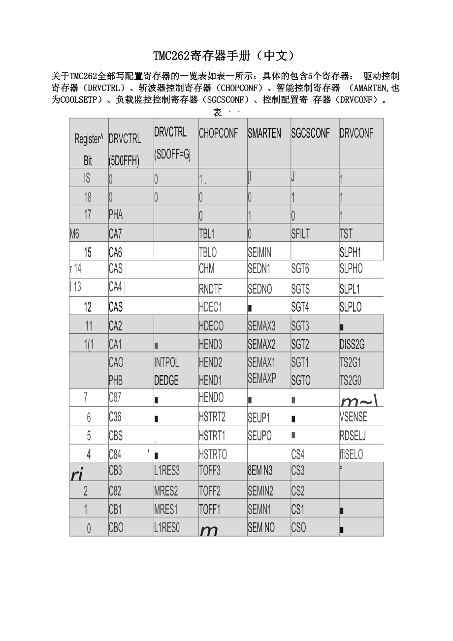
1、TMC262寄存器手册(中文)关于TMC262全部写配置寄存器的一览表如表一所示:具体的包含5个寄存器: 驱动控制寄存器(DRVCTRL)、斩波器控制寄存器(CHOPCONF)、智能控制寄存器 (AMARTEN,也为COOLSETP)、负载监控控制寄存器(SGCSCONF)、控制配置寄 存器(DRVCONF)。表一一RegisterBitDRVCTRL(5D0FFH)DRVCTRL (SDOFF=GjCHOPCONFSMARTENSGCSCONFDRVCONFIS001 .lJ11800 001117PHA0101M6CA7TBL10SFILTTST15CA6TBLOSEIMINSLPH1r
2、14CAS |CHMSEDN1 SGT6SLPHOI 13CA4 |RNDTFSEDNOSGTSSLPL112CASHDEC1SGT4SLPLO11CA2HDECOSEMAX3SGT31(1CA1HEND3SEMAX2SGT2DISS2GCAOINTPOLHEND2SEMAX1SGT1TS2G1PHBDEDGEHEND1SEMAXPSGTOTS2G07C87HENDOm6C36 IHSTRT2SEUP1VSENSE5CBSuHSTRT1SEUPORDSELJ4C84HSTRTOCS4fflSELOriCB3L1RES3TOFF38EM N3CS3*2C82MRES2TOFF2SEMIN2CS2
3、1CB1MRES1TOFF1SEMN1CS10CBOL1RES0mSEM NOCSO1、Driver Control Register (DRVCTRL) 驱动控制寄存器它这里主要分为2种模式SETP/DIR模式与SPI模式,而这2中模式的选择取决于:控制配置寄存器中的:SDOFF mode bit。DRVCTRLDriver Control in STEP/DIR Mode (SDOFF=0)位名字功能注释(Write 000X)190Register add ress bit180Register add ress bit170保留160保留150保留140保留130保留120保留110保
4、留100保留9INTPOLEnable STEP interpolatio n0: Disable STEP pulse interpolation.1: Enable STEP pulse multiplication by 16.STEP信号修改 的使能0:禁止对STEP脉冲信号的插补1:允许,为16clock模式8DEDGEEnable doubl e edgeSTEP pulses0: Rising STEP pulse edge is active, fa lling edge is inactive.1: Both rising and falling STEP pulse e d
5、ges are active.对于STEP信号 脉冲沿方式的 选择0: STEP信号为上升沿有效,下降沿无效。1: STEP信号为双沿有效(上升沿、下降沿都 有效)70保留60保留50保留40保留3MRES3Microstep re solution forSTEP/DIR mo de/微步距进度 配置Microsteps per 90 :%0000: 256%0001: 128%0010: 64%0011: 32%0100: 16%0101: 8%0110: 4 %0111: 2 (halfstep) %1000: 1 (fullstep)2MRES21MRES100001000 共 9 种
6、方式:256,128,64,32,16,8,4,2,10MRESO2、Chopper Control Register (CHOPCONF) 斩波控制寄存器CHOPCONFChopper Configuration位名字功能注释(Write 100X)191Register address b it180Register address b it170Register address b it16TBL1Blanking 廿me斩波的空白时间(也就是关断时 间)此时间需要安全的 覆盖切换事件与持 续的时间去响应检 测电阻Blanking 廿me interval, in system cloc
7、k periods:%00: 16%01: 24%10: 36%11: 5415TBLO设置斩波控制的空白时间00-11,对应16-54 个时钟周期。14CHMChopper mode / 斩波模式的选择This mode bit affects the interpretation of the HDEC, HEND, and HSTRT parameters sho wn below.0 :Standard mode (spreadCycle)1 : Constant tOFF with fast decay 廿me. Fast decay 廿me is also terminated w
8、hen th e negative nominal current is reached. Fast decay is after on 廿me.此位对:HDEC, HEND,HSTRT参数的设置有 影响。0:斩波模式,1:常系数模式,一般选择0。13RNDTFRandom TOFF 廿meEnable randomizing the slow decay phase d ura tion:0: Chopper off 廿me is fixed as set by bits t OFF1: Random mode, tOFF is random modulate d by dNCLK= -12
9、 +3 clocks.随机TOFF时间。0:斩波时间固定1:斩波时间可调12HDEC1Hysteresis decrem entinterval or Fast decay mode磁滞损耗和快速 衰减模式(CHM=0: Hysteresis decreme nt periodset ting, in system clock periods:%00: 16%01: 32%10: 48%11: 64)(CHM=1: HDEC1=0:current comparator can te rmin ate the fast decay phase before 廿 mer e xpires.HDEC
10、1=1: only the 廿 mer term in ates the fast decay phase.HDEC0: MSB of fast decay 廿me setting.)11HDECOCHM=0:磁滞衰减周期设置:00:11: 16,32, 48, 64CHM=1常系数模式设置:HDEC1=1禁止电流比较器作为快衰减的终止HDEC0:快衰减的时间最高位设置10HEND3Hysteresis end (lo w) value or Sine wave offset/ 迟滞低位值或者正 弦波偏置CHM=0:%0000 %1111:Hysteresis is -3, -2, -1, 0
11、, 1,,12 (1/512 of this set ting adds to curre nt set tin g) This is the hysteresis value which becom es used for the hysteresis chopper.CHM=1:%0000 %1111: Offset is -3,-乙-1,0, 1,,12 ,This is the sine wave offset and 1/512 of the value becomes added to the absolute value of each sine wave entry.9HEND
12、28HEND10000: 1111:迟滞为-3,-212,当CHM=1时,这个表示正弦波偏置7HENDO6HSTRT2Hysteresis start va lue orFast decay 廿me Setti ng / 迟滞开始值或快衰 时间设置CHM=0: Hysteresis start offset from HEND:%000: 1%100:5%001: 2 %101: 6%010: 3%110:7%011: 4%111:8Effective: HEND+HSTRT must be W 15 CHM=1 :Three least-significant bits of the dur
13、ation of the fast decay phase. The MSB isHDEC0. Fast decay 廿me is a multiple of system clockperiods: NCLK= 32 x (HDEC0+HSTRT)5HSTRT14HSTRTOCHM=0: DAC迟滞设置000011:对应的HEND 增力口 5, 68且 HEND+HSTRT mustbe W 15才有效。CHM=1 :快衰时间设置。NCLK= 32 x (HDEC0+HSTRT)3TOFF3Off 廿me/MOSFET disable /off 廿me 驱动使能(斩波慢 衰减时间,影响开 关
14、频率)控制着慢 衰减时间的持续时 间,并控制着斩波 的最大频率Duration of slow decay phase. If TOFF is 0, the MOSFETs are shut off. If TOFF isnon zero, slow decay 廿me is a mul ti ple of s ystem clock periods:NCLK= 12 + (32 x TOFF) (Minimum 廿me is 64clocks.)%0000: Driver disable, all bridges off%0001: 1 (use with TBL of minimum 24
15、 clo cks)%0010 %1111: 2 152TOFF21TOFF10000:禁止所有驱动器晶体管,电机可以自由 转0001: TBL最小24个时钟周期00101111: 2150TOFFO3、coolStep Control Register (SMARTEN)智能控制寄存器SMAR TENChopper Configuration位名字功能注释(Write 1010X)191Register address bit180Register address bit171Register address bit160保留15SEIMINMinimum coolStep current /
16、 智能电流控制的最小电 流0: % CS current setting 1: % CS current setting0:设置电流的1/21:设置电流的1414SEDN1Current decrement speed / 智能电流的减少速度Number of times that the stallGuard2 value mus t be sampled equal to or above the upper thre shold for each decrement of the coil current: %00: 32%01: 8%10: 2%11: 113SEDN000:每32个负
17、载衰减值电流减小一个单位 01 :每8个负载衰减值电流减小一个单位 10:每2个负载衰减值电流减小一个单位 11:每个负载衰减值电流减小一个单位120保留11SEMAX3Upper coolStep threshold as an offset from the lower threshold / 最小电流控制时负载 的磁滞值(高位安全门 限)If the stallGuard2 measurement value SG is sam pled equal to or above (SEMIN+SEMAX+1) x 32 enough times, then the coil current
18、scaling facto r is decremented.10SEMAX29SEMAX18SEMAX0如果负载检测值三(SEMIN+SEMAX+1)*32电机电流回到安全值。00001111: 01570保留6SEUP1Current increment size / 智能电流的增加速度Number of current increment steps for each tim e that the stallGuard2 value SG is sampled belo w the lower threshold:%00: 1%01: 2%10: 4%11: 85SEUPO每个负载测量值
19、:0011: 1,2,4,840保留3SEMIN3Lower coolStep threshold/coolStep disable ) /智能电流控制的最小 负载检测值和电流使 能If SEMIN is 0, coolStep is disabled. If SEMIN is nonzero and the stallGuard2 value SG fallsbelow SEMIN x 32, the coolStep current scalingfactor is increased.2SEMIN21SEMIN10000:禁止电流控制如果负载检测值V SEMIN*32,电机电流减小,负
20、载转动角度将增加。00011111: 0150SEMINO4、stallGuard2 Control Register (SGCSCONF) 负载监控控制寄 存器SMARTENChopper Configuration位名字功能注释(Write 110X)191Register address bit181Register address bit170Register address bit16SFILTstallGuard2 filter en able负载检测滤波使能0: Standard mode, fastest response 廿me. 1: Filtered mode, upda
21、ted once for each four fullsteps to compensate for variation in motor construction, highest accuracy.0:标准模式,最快的响应速度。1:滤波模式:每4个整步时信号偏差才补 偿,最高时间精度150保留14SGT6stallGuard2 threshold value /负载阀值的设定The stallGuard2 threshold value controls the optimum measurement range for rea dout and stall indicator outpu
22、t (SG_TST). A lower value results in a higher sen si tivity and less torque is required to i ndicate a stall. The value is a two s com plement signed integer. Values below -10 are not recommended. Range: -64 to +6313SGT512SGT4这里的信号值控制负载的阀值输出,为输出 设置最优化的边界,设定值越低,灵敏度越 咼,0为大部分电机的工作开始值,设定值 越高,灵敏度越低,需要更低转
23、矩来决定负 载值,不建议小于-10。11SGT310SGT29SGT18SGT070保留60保留50保留4CS4Current scale(scales digital currents A and B) / 电流的标准A相或B 相Current scaling for SPI and STEP/DIR opera 廿on. %00000 %11111: 1/32, 2/32, 3/32,32/32 This value is biased by 1 anddi vided by 32, so the range is 1/32 to 32/3 2.Example: CS=20 is 21/3
24、2 current.3CS32CS21CS1驱动电流0-3100001111 ;分别对应1/3232/320CS05、Driver Control Register (DRVCONF) 驱动配置寄存器DRVCONFDriver Configuration位名字功能注释(Write 111X)191Register address bit181Register address bit171Register address bit16TSTReserved TEST mode / 为测试模式保留Must be cleared for normal operation. When set, the
25、SG_TST output exposes digital test values, and the TEST_ANA output exposes analog test values. Test value selection is controlled by SGT1 and SGT0:TEST_ANA: %00: anatest_2vth,%01: anatest_dac_out,%10: anatest_vdd_half.SG_TST:%00: comp_A,%01: comp_B,%10: CLK,%11: on state xy测试的时候必须清除的正常运行,设置为0,当设 置为1
26、时,SG_TST输出数字测试值,TEST_ANA输 出模拟测试值,输出测试值的选择由SGT1 andSGT0所决定。15SLPH1Slope control, high side / 上功率管控制斜率%00: Minimum%01: Minimum temperature compensation mode. %10: Medium temperature compensation mode. %11: MaximumIn temperature compensated mode (tc), the MOSFET gate driver strength is increased if the
27、 overtemperature warning temperature is reached.This compensates for temperature dependency of high-side slope control.14SLPH000:最小值,01 :最小的温度补偿模式,10:中间值的温度补偿模式11:最大值在温度补偿模式中,随着温度的增加对MOSFET门 级的驱动电流是增加的,如果超过警戒电流,温度 的补偿模式会依靠上功率管斜率控制进行控制13SLPL1Slope control, low side/下功率管控制斜率%00: Minimum.%01: Minimum.%
28、10: Medium.%11: Maximum.12SLPL000&01 :最小值,10:中间值,11:最大值110保留10DISS2GShort to GND protection disable / 短接到地保护使能0: Short to GND protection is enabled. 1: Short to GND protection is disabled.0:使能,1:非使能9TS2G1Short to GND detection timer /短接到地保护时间%00: 3.2ys.%01: 1.6ys.%10: 1.2ys.%11: 0.8ys.8TS2G07SDOFFST
29、EP/DIR interface disable /STEP/DIR 与 SPI 模式的选择0: Enable STEP/DIR operation.1: Disable STEP/DIR operation. SPI interface is us ed to move motor.0: STEP/DIR模式;1: SPI 模式6VSENSESense resistor voltage-based current scaling /检测参考电压的边界0: Full-scale sense resistor voltage is 305mV. 1: Full-scale sense resis
30、tor voltage is 165mV. (Full-scale refers to a current setting of 31 and a DAC value of 255.)0: 采样电压值最大305mV,1:采样电压值最大165mV5RDSEL1Select value for read out (RD bits) / 读取返回项%00 Microstep position read back%01 stallGuard2 level read back%10 stallGuard2 and coolStep current level read back%11 Reserved,
31、 do not use4RDSEL000:返回微步位置,01:返回负载值,10: 读回负载和智能电流级别,11:保留,未使用30保留20保留10保留00保留6、Read Response 读响应寄存器DRVSTATUSRead Response位名字功能注释RDSEL=%00%01%1019MSTEP9SG9SG9Microstep counter f or coil AorstallGuard2 value SG9:0orstallGuard2 value SMicrostep position in sine table for coil A in STEP/DIR mode. MSTEP
32、9 is the Polarity bit:0:Current flows from OA1 pins to OA2 pins.1:Current flows from OA2 pins to OA1 pins. /18MSTEP8SG8SG817MSTEP7SG7SG716MSTEP6SG6SG6G9:5 AndcoolStep valueSE4:0/一共有二种功能:1、 返回A相在微步时 的正弦列表值;2、负载测试的0- 9位;3、负载测试的9-5 位以及电流控制值tallGuard2 value SG9:0. / stallGuard2 value SG9:5 and the act u
33、alcoolStep scaling value SE4:0.15MSTEP5SG5SG514MSTEP4SG4SE4RDSEL=00:左示功能 1,RDSEL=01: 左示功能2 RDSEL=10:左示功能313MSTEP3SG3SE312MSTEP2SG2SE211MSTEP1SG1SE110MSTEP0SG0SE090807STSTStandstill indicator步进保持指示0: No standstill condition detected 1: No active edge occurred on theSTEP input during the last 2A20 sys
34、tem clock cycles.0:没有达到步进检测的条件1:指示在最近2八20次方时钟周期内没有步进脉冲6OLBOpen load indicator / 开路负载指示0:No open load conditiondetected.1: No chopper event has happened duringthe last period with constant coil polarity. Only a current above 1/16 of the maximum setting can clear this bit!Hint: This bit is only a stat
35、us indicator. The chip takes no other action when this bit is set. False indications may occur during fast motion and at standstill. Check this bit only during slow motion.5OLA0:无开路负载时。无斩波动作时为1, 当有一个电流的最大设定值的1/16以 上时,可以清除该位!注意:该位仅 在一个状态指示灯。该芯片采取其他任何行动时,该位被设置。假的标志 可能会出现在快速运动和静止状态。 检查该位只在慢动作。4S2GBShor
36、t to GND detection bits on high-side transistors/高端晶体管短路到 地0:No short to ground shutdowncondition.1:Short to ground shutdown condition.The short counter is incremented by each short circuit and the chop per cycle is suspended. The counter is decremented for each phase pola rity change. The MOSFETs a
37、re shut off when the counter reaches 3 and remain shut off until the shutdown condition is cleared by di sabling and re-enabling the driver. T he shutdown condition becomes reset by deasserting the ENN input or clearing the TOFF parameter.3S2GA0:没有短到地关机状态。 1:短到地面关机状态。每个短路计数器的递增状态是由每个 短路电流的周期和斩波周期所决定
38、 的;每当相位的极性发生变化时,计 数器实行递减。短路发生后,斩波终 止,短路计数,器加一,当发生3次 时,需要复位才能启动驱动器。 通过置ENN为无效的操作或者清除 TOFF参数来使关机状态置为复位状 态2OTPWOvertemperature war ning./过温警告0:No overtemperature warningcondition.1:Warning threshold is active.0:没有达到超温警报条件1:过温警告有效1OTOvertemperature shutdown/过热关机0:No overtemperature shutdowncondition.1: Overtemperature shutdown has occurred. occurred.0:没有达到过热关机条件1:过热关机有效0SGstallGuard2 status/负载状态0:No motor stall detected.1:stallGuard2 threshold has beenreached and theoutput is driven high.0:未检测到电机负载1超过负载阀值,并且SG_TST输出 高电平
- 温馨提示:
1: 本站所有资源如无特殊说明,都需要本地电脑安装OFFICE2007和PDF阅读器。图纸软件为CAD,CAXA,PROE,UG,SolidWorks等.压缩文件请下载最新的WinRAR软件解压。
2: 本站的文档不包含任何第三方提供的附件图纸等,如果需要附件,请联系上传者。文件的所有权益归上传用户所有。
3.本站RAR压缩包中若带图纸,网页内容里面会有图纸预览,若没有图纸预览就没有图纸。
4. 未经权益所有人同意不得将文件中的内容挪作商业或盈利用途。
5. 装配图网仅提供信息存储空间,仅对用户上传内容的表现方式做保护处理,对用户上传分享的文档内容本身不做任何修改或编辑,并不能对任何下载内容负责。
6. 下载文件中如有侵权或不适当内容,请与我们联系,我们立即纠正。
7. 本站不保证下载资源的准确性、安全性和完整性, 同时也不承担用户因使用这些下载资源对自己和他人造成任何形式的伤害或损失。
