 高精度低成本电流源使用AD8276差分放大器和AD8603运算放大器

《高精度低成本电流源使用AD8276差分放大器和AD8603运算放大器》由会员分享,可在线阅读,更多相关《高精度低成本电流源使用AD8276差分放大器和AD8603运算放大器(18页珍藏版)》请在装配图网上搜索。
1、高精度,低成本电流源使用AD8276差分放大器和AD8603运算放大器 电流源广泛用于工业、通信和其它设备中的传感器激励和设备间通信等领域。例如,过程控制设备中广泛采用的4 mA至20 mA环路。利用DAC、放大器(运算放大器或差动放大器)和匹配电阻,可以构建可编程电流源。低值电流源可以集成到低输出电流源或放大器中。例如,仪表放大器AD8290内部集成一个电流源,高分辨率- ADCAD7794 具有两个集成电流源。对于较大电流,一般需要外部MOSFET或晶体管。利用低功耗差动放大器AD8276和运算放大器AD8603构建的电流源,不仅经济、灵活、小巧,而且初始误差、温度漂移和功耗等性能也都非常
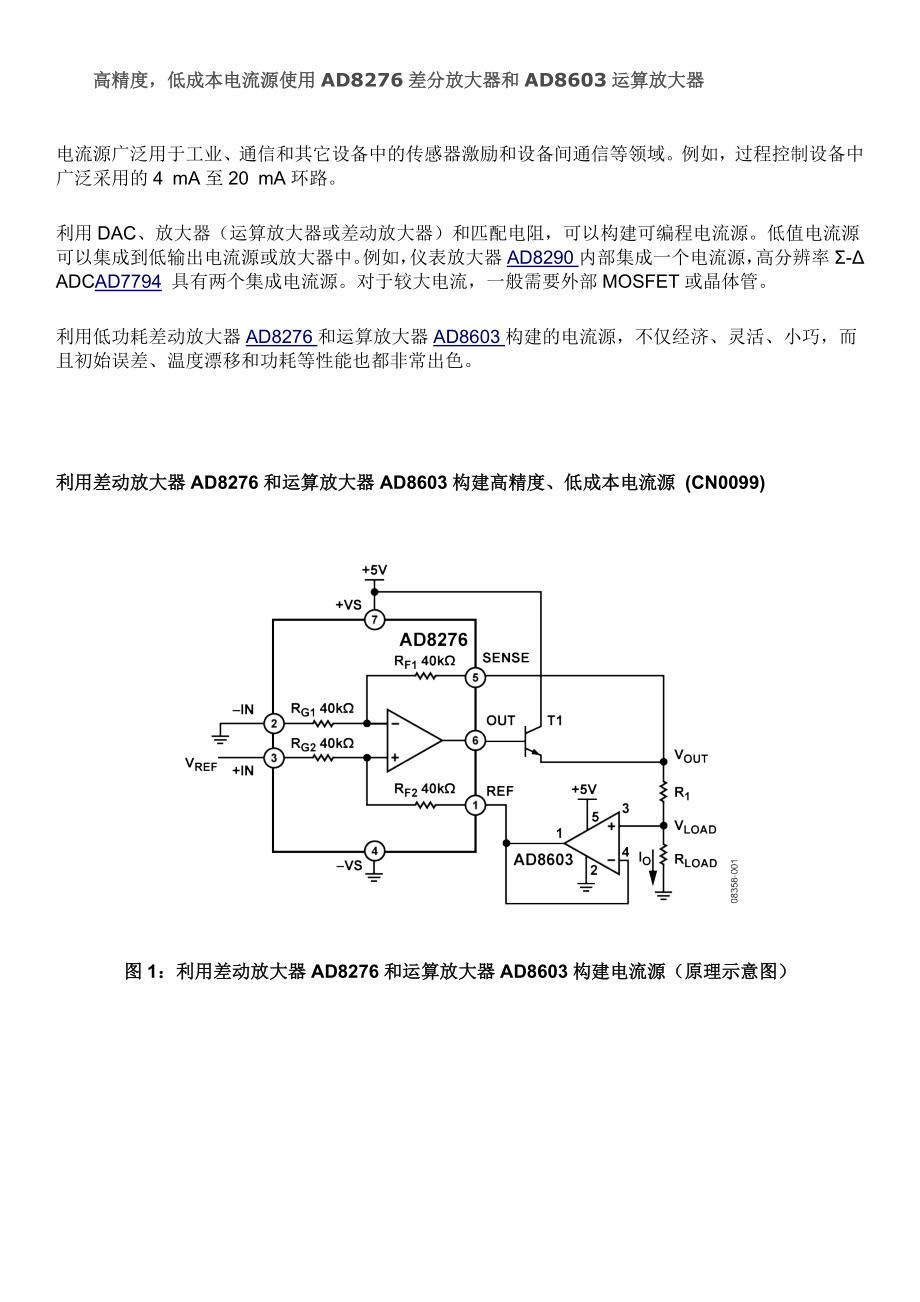
2、出色。利用差动放大器AD8276和运算放大器AD8603构建高精度、低成本电流源 (CN0099) 图1:利用差动放大器AD8276和运算放大器AD8603构建电流源(原理示意图)图1:利用差动放大器AD8276和运算放大器AD8603构建电流源(原理示意图) 电路描述 电流源电路如图1所示。基准电压VREF加在AD8276的同相输入端,该电压控制输出电流量 IO。 AD8276的反相输入端则直接接地。该器件内置四个40 k激光调整电阻,分别与输入引脚、REF引脚和SENSE引脚相连。如果需要高电流输出,则AD8276的输出可用来驱动一个晶体管。如果电阻完全匹配,R1上的电压即输入电压VREF
3、,从而产生恒定的负载电流IO,它等于VREF/R1。由于运算放大器AD8603具有低偏置电流源广泛用于工业、通信和其它设备中的传感器激励和设备间通信等领域。例如,过程控制设备中广泛采用的4 mA至20 mA环路。利用DAC、放大器(运算放大器或差动放大器)和匹配电阻,可以构建可编程电流源。低值电流源可以集成到低输出电流源或放大器中。例如,仪表放大器AD8290内部集成一个电流源,高分辨率- ADCAD7794 具有两个集成电流源。对于较大电流,一般需要外部MOSFET或晶体管。利用低功耗差动放大器AD8276和运算放大器AD8603构建的电流源,不仅经济、灵活、小巧,而且初始误差、温度漂移和功
4、耗等性能也都非常出色。利用差动放大器AD8276和运算放大器AD8603构建高精度、低成本电流源 (CN0099) 图1:利用差动放大器AD8276和运算放大器AD8603构建电流源(原理示意图)图1:利用差动放大器AD8276和运算放大器AD8603构建电流源(原理示意图) 电路描述 电流源电路如图1所示。基准电压VREF加在AD8276的同相输入端,该电压控制输出电流量 IO。 AD8276的反相输入端则直接接地。该器件内置四个40 k激光调整电阻,分别与输入引脚、REF引脚和SENSE引脚相连。如果需要高电流输出,则AD8276的输出可用来驱动一个晶体管。如果电阻完全匹配,R1上的电压即
5、输入电压VREF,从而产生恒定的负载电流IO,它等于VREF/R1。由于运算放大器AD8603具有低偏置电流(最大值为1 pA)和低失调电压(小于50 V)特性,所以在电路的反馈环路中选用该器件。低偏置电流特性使它能与高阻抗负载接口,而不会引入明显的失调误差。低温度漂移特性(最大值为4.5 V/C)使它能在较宽的温度范围内工作,而且该放大器还具有低噪声以及轨到轨输入和输出特性。输出电流值IO可通过下式计算:AD8276具有非常严格的电阻匹配,RF1/RG1 = RF2/RG2 = 1,因此公式1可简化为: 公式1显示,图1所示电路的主要误差源于内部电阻匹配、R1的公差和负载电阻的公差。AD82
6、76(B级)的最大增益误差为0.02%,AD8276(A级)的最大增益误差为0.05%,该电路的整体精度可以达到0.02%。同时,R1的精度也非常重要,其公差应达到0.1%或更佳,此误差可通过校准来消除。电路的输出电流量IO受以下因素限制:运算放大器输入范围、差动放大器输出范围以及差动放大器SENSE引脚电压范围。根据图1,必须满足以下三个条件: 1. VLOAD = IO RLOAD 必须在运算放大器AD8603的输入范围内。2. VOUT = IO (RLOAD + R1) 必须在AD8276 SENSE引脚电压范围内:2(?Vs) ? 0.2 V 至 2(+Vs) ? 3 V.3. IO
7、 (RLOAD + R1) + 2(?Vs) ? 0.2 V 至 2(+Vs) ? 3 V 必须在AD8276输出电压范围内:Vs + 0.2 V 至 +Vs ? 0.2 V.AD8276具有轨到轨输出特性,可采用2.5 V至36 V电源供电,因而输出电流范围较宽。 AD8276B的最大失调电压漂移为2 V/C,最大增益漂移为1 ppm/C,温度漂移较低,工作温度范围较宽。AD8276A的最大失调电压漂移和最大增益漂移分别为5 V/C和5 ppm/C。AD8276(8引脚MSOP)和AD8603(5引脚TSOT-23)均采用小尺寸封装,因此该电路所需的电路板面积极小。外部电流源晶体管T1的击穿
8、电压VCB应高于AD8276电源电压。该晶体管的最大集电极电流应高于预期的输出电流并具有适当的裕量,而且必须遵循晶体管功耗限制。推荐使用2N3904、2N4401、2N3391和MPSA06等低成本晶体管。AD8276可以驱动15 mA以下的输出电流,而不需要外部晶体管或MOSFET。图2所示为室温下采用AD8276A、AD8603和2N3904的测试结果。R1为50 ,公差0.1%。显然,实际输出与计算结果相符。在所示数值范围内,测量结果与理想结果相差无几,不超过0.5%,平均误差低于R1公差限制的0.1%。 利用差动放大器AD8276和运算放大器AD8603构建高精度、低成本电流源 (CN
9、0099) 图2:利用AD8276A、AD8603和2N3904构建的电流源测试结果(R1 = 50 ,RLOAD = 100 ,Vs = +5 V,TA = 25C)图2:利用AD8276A、AD8603和2N3904构建的电流源测试结果(R1 = 50 ,RLOAD = 100 ,Vs = +5 V,TA = 25C) 与其它高精度电路一样,必须采用适当的布局、接地和去耦技术。欲了解更多信息,请参考 教程 MT-031“实现数据转换器的接地并解开AGND和DGND的谜团”,以及教程MT-101“去耦技术”。常见变化 如果需要更高的电源,以获得更高的输出电流值,可以使用OP1177、AD86
10、61和AD8663。重要特性包括电源电压范围、偏置电流、失调电压、输入电压范围和温度漂移。如果需要固定电流源,则VREF 可以由基准电压源提供,例如ADR36x 系列。ADR82x系列集成基准电压源和运算放大器,可采用最高36 V的电源供电,从而可进一步节省空间。如果需要双通道电流源,AD8607 和AD8277 都是不错的选择。如果需要可编程电流源,请使用精密14位或16位DAC来产生基准电压VREF。AD5560、AD5060 (单通道)和AD5663R (双通道)均适合这种应用。电流(最大值为1 pA)和低失调电压(小于50 V)特性,所以在电路的反馈环路中选用该器件。低偏置电流特性使它
11、能与高阻抗负载接口,而不会引入明显的失调误差。低温度漂移特性(最大值为4.5 V/C)使它能在较宽的温度范围内工作,而且该放大器还具有低噪声以及轨到轨输入和输出特性。输出电流值IO可通过下式计算:AD8276具有非常严格的电阻匹配,RF1/RG1 = RF2/RG2 = 1,因此公式1可简化为: 公式1显示,图1所示电路的主要误差源于内部电阻匹配、R1的公差和负载电阻的公差。AD8276(B级)的最大增益误差为0.02%,AD8276(A级)的最大增益误差为0.05%,该电路的整体精度可以达到0.02%。同时,R1的精度也非常重要,其公差应达到0.1%或更佳,此误差可通过校准来消除。电路的输出
12、电流量IO受以下因素限制:运算放大器输入范围、差动放大器输出范围以及差动放大器SENSE引脚电压范围。根据图1,必须满足以下三个条件: 1. VLOAD = IO RLOAD 必须在运算放大器AD8603的输入范围内。2. VOUT = IO (RLOAD + R1) 必须在AD8276 SENSE引脚电压范围内:2(?Vs) ? 0.2 V 至 2(+Vs) ? 3 V.3. IO (RLOAD + R1) + 2(?Vs) ? 0.2 V 至 2(+Vs) ? 3 V 必须在AD8276输出电压范围内:Vs + 0.2 V 至 +Vs ? 0.2 V.AD8276具有轨到轨输出特性,可采用
13、2.5 V至36 V电源供电,因而输出电流范围较宽。 AD8276B的最大失调电压漂移为2 V/C,最大增益漂移为1 ppm/C,温度漂移较低,工作温度范围较宽。AD8276A的最大失调电压漂移和最大增益漂移分别为5 V/C和5 ppm/C。AD8276(8引脚MSOP)和AD8603(5引脚TSOT-23)均采用小尺寸封装,因此该电路所需的电路板面积极小。外部电流源晶体管T1的击穿电压VCB应高于AD8276电源电压。该晶体管的最大集电极电流应高于预期的输出电流并具有适当的裕量,而且必须遵循晶体管功耗限制。推荐使用2N3904、2N4401、2N3391和MPSA06等低成本晶体管。AD82
14、76可以驱动15 mA以下的输出电流,而不需要外部晶体管或MOSFET。图2所示为室温下采用AD8276A、AD8603和2N3904的测试结果。R1为50 ,公差0.1%。显然,实际输出与计算结果相符。在所示数值范围内,测量结果与理想结果相差无几,不超过0.5%,平均误差低于R1公差限制的0.1%。 利用差动放大器AD8276和运算放大器AD8603构建高精度、低成本电流源 (CN0099) 图2:利用AD8276A、AD8603和2N3904构建的电流源测试结果(R1 = 50 ,RLOAD = 100 ,Vs = +5 V,TA = 25C)图2:利用AD8276A、AD8603和2N3
15、904构建的电流源测试结果(R1 = 50 ,RLOAD = 100 ,Vs = +5 V,TA = 25C) 与其它高精度电路一样,必须采用适当的布局、接地和去耦技术。欲了解更多信息,请参考 教程 MT-031“实现数据转换器的接地并解开AGND和DGND的谜团”,以及教程MT-101“去耦技术”。常见变化 如果需要更高的电源,以获得更高的输出电流值,可以使用OP1177、AD8661和AD8663。重要特性包括电源电压范围、偏置电流、失调电压、输入电压范围和温度漂移。如果需要固定电流源,则VREF 可以由基准电压源提供,例如ADR36x 系列。ADR82x系列集成基准电压源和运算放大器,可
16、采用最高36 V的电源供电,从而可进一步节省空间。如果需要双通道电流源,AD8607 和AD8277 都是不错的选择。如果需要可编程电流源,请使用精密14位或16位DAC来产生基准电压VREF。AD5560、AD5060 (单通道)和AD5663R (双通道)均适合这种应用。Circuit Function and Benefits Current sources are widely used in industrial, communication, and other equipment for sensor excitation and machine-to-machine commu
17、nication, etc. For example, the 4 mA-to-20 mA loop is widely used in process control equipment.Programmable current sources can be built using a DAC, amplifier (op amp or difference amplifier), and matched resistors. Low value current sources can be integrated into low output current sources or ampl
18、ifiers. For example, the AD8290 is an instrumentation amplifier with a single integrated current source, and the AD7794 is a high resolution - ADC with two integrated current sources. For high currents, external MOSFETs or transistors will generally be required.Current sources using the low power AD
19、8276 difference amplifier and the AD8603 op amp are affordable, flexible, and small in size. Performance characteristics such as initial error, temperature drift, and power dissipation are excellent.High Precision, Low Cost Current Sources Using the AD8276 Difference Amplifier and the AD8603 Op Amp
20、(CN0099) Figure 1: Current Source Using the AD8276 Difference Amplifier and the AD8603 Op Amp (Simplified Schematic)Figure 1: Current Source Using the AD8276 Difference Amplifier and the AD8603 Op Amp (Simplified Schematic) Circuit Description The current source circuit is shown in Figure 1. Referen
21、ce voltage, VREF, is applied to the noninverting input of the AD8276. This voltage controls the amount of output current, IO. The inverting input of the AD8276 is connected directly to ground. There are four laser-trimmed, 40 k resistors inside the AD8276 that are connected to the input pins, the RE
22、F pin, and the SENSE pin. The output of the AD8276 is used to drive a transistor if a high current output is needed.If the resistors are perfectly matched, the input voltage, VREF, appears across R1, thereby producing a constant load current, IO, which is equal to VREF/R1.The AD8603 op amp is used i
23、n the feedback loop of the circuit and was chosen because of its low bias current (maximum 1 pA) and offset voltage (less than 50 V). The low bias current makes it possible to interface to a high impedance load without introducing significant offset errors. The AD8603 low temperature drift specifica
24、tion (4.5 V/C maximum) allows operation over a wide temperature range, and the amplifier also features low noise and rail-to-rail inputs and outputs.The value of the output current, IO, can be calculated by using the equationBecause the AD8276 has very tight resistor matching, RF1/RG1 = RF2/RG2 = 1,
25、 and Equation 1 can be simplified as Equation 1 shows that the primary errors of the circuit in Figure 1 are due to the internal resistor matching, the tolerance of R1, and the tolerance of the load resistance. The AD8276 (B-grade) maximum gain error is 0.02%. The AD8276 (A-grade) maximum gain error
26、 is 0.05%. Overall accuracy of 0.02% is possible with the circuit.At the same time, the accuracy of R1 is critical, so it should have 0.1% tolerance or better. This error can be removed by calibration.The amount of output current, IO, available from the circuit is limited by the op amp input range,
27、the difference amplifier output range, and the difference amp SENSE pin voltage range.Based on Figure 1, three conditions have to be met: 1. VLOAD = IO RLOAD must be within the AD8603 op amp input range.2. VOUT = IO (RLOAD + R1) must be within the AD8276 SENSE pin voltage range: 2(Vs) 0.2 V to 2(+Vs
28、) 3 V.3. IO (RLOAD + R1) + 2(Vs) 0.2 V to 2(+Vs) 3 V must be within the AD8276 output voltage range: Vs + 0.2 V to +Vs 0.2 V.The AD8276 rail-to-rail output feature and the ability to operate on a 2.5 V to 36 V power supply allow a wide range of output current. The AD8276B offset voltage drift of 2 V
29、/C maximum and gain drift of 1 ppm/C maximum yield low temperature drift and wide temperature operation. The specifications for the AD8276A are 5 V/C and 5 ppm/C, respectively.Both the AD8276 (8-lead MSOP) and the AD8603 (5-lead TSOT-23) are in small packages, thereby minimizing the board area requi
30、red by the circuit.The external current source transistor, T1, should have a VCB breakdown voltage higher than the AD8276 supply voltage. The transistor maximum collector current should be higher than the expected output current with suitable headroom, and the transistor power dissipation limits mus
31、t be observed. Low cost transistors, such as the 2N3904, 2N4401, 2N3391, and MPSA06 are recommended.The AD8276 can drive output currents of 15 mA or less without the need for the external transistor or MOSFET.Testing results under room temperature based on theAD8276A, AD8603, and 2N3904 are shown in
32、 Figure 2. R1 is 50 with 0.1% tolerance. It is obvious that the actual output complies with the calculated results. On the scale shown, the measured results are indistinguishable from the ideal results because they are within 0.5% of each other with the average of less than 0.1% limited by the R1s t
33、olerance.High Precision, Low Cost Current Sources Using the AD8276 Difference Amplifier and the AD8603 Op Amp (CN0099) Figure 2: Test Results for Current Source Using the AD8276A, AD8603, and 2N3904 (R1 = 50 , RLOAD = 100 , Vs = +5 V, TA = 25C)Figure 2: Test Results for Current Source Using the AD82
34、76A, AD8603, and 2N3904 (R1 = 50 , RLOAD = 100 , Vs = +5 V, TA = 25C) As with any high accuracy circuit, proper layout, grounding, and decoupling techniques must be employed. See Tutorial MT-031, Grounding Data Converters and Solving the Mystery of AGND and DGND and Tutorial MT-101, Decoupling Techn
35、iques for more details.Common Variations If higher power supplies are needed for higher value output current, the OP1177, AD8661, and AD8663 can be used. The important specifications are power supply range, bias current, offset voltage, input voltage range, and temperature drift.If a fixed current s
36、ource is required, VREF can be supplied by a voltage reference such as the ADR36x family.The ADR82x family integrates a voltage reference and an op amp and can operate on a power supply up to 36 V. This provides an additional space saving option.If a dual-current source is needed, the AD8607 and the are good choices.If programmable current sources are needed, use a precision 14-bit or 16-bit DAC to generate the reference voltage, VREF. The AD5560, AD5060 (single), and AD5663R (dual) are suitable for this application.
- 温馨提示:
1: 本站所有资源如无特殊说明,都需要本地电脑安装OFFICE2007和PDF阅读器。图纸软件为CAD,CAXA,PROE,UG,SolidWorks等.压缩文件请下载最新的WinRAR软件解压。
2: 本站的文档不包含任何第三方提供的附件图纸等,如果需要附件,请联系上传者。文件的所有权益归上传用户所有。
3.本站RAR压缩包中若带图纸,网页内容里面会有图纸预览,若没有图纸预览就没有图纸。
4. 未经权益所有人同意不得将文件中的内容挪作商业或盈利用途。
5. 装配图网仅提供信息存储空间,仅对用户上传内容的表现方式做保护处理,对用户上传分享的文档内容本身不做任何修改或编辑,并不能对任何下载内容负责。
6. 下载文件中如有侵权或不适当内容,请与我们联系,我们立即纠正。
7. 本站不保证下载资源的准确性、安全性和完整性, 同时也不承担用户因使用这些下载资源对自己和他人造成任何形式的伤害或损失。
最新文档
- 部编人教版语文三年级下册第八单元 方帽子店 ppt课件
- 微生物灭菌问题培训课件
- 廊坊房地产市场整合课件
- 廖小菲XXXX财务报告—利润表-课件
- 廊坊售后11月目标完成报告课件
- 部编人教版四年级语文上册《口语交际 我们与环境》优质ppt课件
- 延伸存取列表课件
- 部编人教版语文三年级下册第六单元 习作:身边那些有特点的人 ppt课件
- 廉颇蔺相如列传重点语句翻译上课-课件
- 廉颇蔺相如列传课件
- 廉颇蔺相如列传公开课优质课-课件
- 微生物活菌计数方法教学课件
- 部编人教版三年级数学下册第4课时 简单的路线图课件
- 廉洁行医秉公奉廉医疗卫生行业廉洁自律培训模板课件
- 部编人教版六年级道德与法制上册第8课《我们受特殊保护》 ppt课件完整版
![广西北海市医疗保障事业管理中心招考聘用就业见习生(同步测试)模拟卷含答案[8]](/Images/s.gif)