 Microsemi IGL002 FPGA系列开发方案

《Microsemi IGL002 FPGA系列开发方案》由会员分享,可在线阅读,更多相关《Microsemi IGL002 FPGA系列开发方案(19页珍藏版)》请在装配图网上搜索。
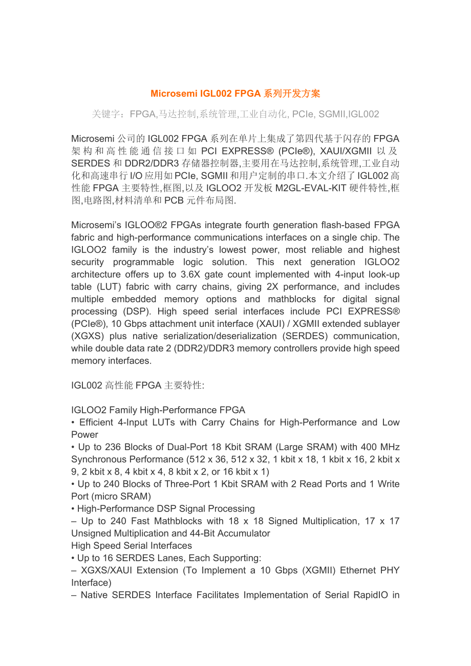
1、Microsemi IGL002 FPGA系列开发方案关键字:FPGA,马达控制,系统管理,工业自动化, PCIe, SGMII,IGL002Microsemi公司的IGL002 FPGA系列在单片上集成了第四代基于闪存的FPGA架构和高性能通信接口如PCI EXPRESS (PCIe), XAUI/XGMII以及SERDES和DDR2/DDR3存储器控制器,主要用在马达控制,系统管理,工业自动化和高速串行I/O应用如PCIe, SGMII和用户定制的串口.本文介绍了IGL002高性能FPGA主要特性,框图,以及IGLOO2开发板M2GL-EVAL-KIT硬件特性,框图,电路图,材料清单和PC
2、B元件布局图.Microsemis IGLOO2 FPGAs integrate fourth generation flash-based FPGA fabric and high-performance communications interfaces on a single chip. The IGLOO2 family is the industrys lowest power, most reliable and highest security programmable logic solution. This next generation IGLOO2 architectur
3、e offers up to 3.6X gate count implemented with 4-input look-up table (LUT) fabric with carry chains, giving 2X performance, and includes multiple embedded memory options and mathblocks for digital signal processing (DSP). High speed serial interfaces include PCI EXPRESS (PCIe), 10 Gbps attachment u
4、nit interface (XAUI) / XGMII extended sublayer (XGXS) plus native serialization/deserialization (SERDES) communication, while double data rate 2 (DDR2)/DDR3 memory controllers provide high speed memory interfaces.IGL002高性能FPGA主要特性:IGLOO2 Family High-Performance FPGA Efficient 4-Input LUTs with Carry
5、 Chains for High-Performance and Low Power Up to 236 Blocks of Dual-Port 18 Kbit SRAM (Large SRAM) with 400 MHz Synchronous Performance (512 x 36, 512 x 32, 1 kbit x 18, 1 kbit x 16, 2 kbit x 9, 2 kbit x 8, 4 kbit x 4, 8 kbit x 2, or 16 kbit x 1) Up to 240 Blocks of Three-Port 1 Kbit SRAM with 2 Rea
6、d Ports and 1 Write Port (micro SRAM) High-Performance DSP Signal Processing Up to 240 Fast Mathblocks with 18 x 18 Signed Multiplication, 17 x 17 Unsigned Multiplication and 44-Bit AccumulatorHigh Speed Serial Interfaces Up to 16 SERDES Lanes, Each Supporting: XGXS/XAUI Extension (To Implement a 10
7、 Gbps (XGMII) Ethernet PHY Interface) Native SERDES Interface Facilitates Implementation of Serial RapidIO in Fabric or an SGMII Interface to a soft Ethernet MAC PCI Express (PCIe) Endpoint Controller x1, x2, x4 Lane PCI Express CoreUp to 2 Kbytes Maximum Payload Size64-/32-Bit AXI/AHB Master and Sl
8、ave Interfaces to the Application LayerHigh Speed Memory Interfaces Up to 2 High Speed DDRx Memory Controllers HPMS DDR (MDDR) and Fabric DDR (FDDR) Controllers Supports LPDDR/DDR2/DDR3 Maximum 333 MHz Clock Rate SECDED Enable/Disable Feature Supports Various DRAM Bus Width Modes, x8, x9, x16, x18,
9、x32, x36 Supports Command Reordering to Optimize Memory Efficiency Supports Data Reordering, Returning Critical Word First for Each Command SDRAM Support through a Soft SDRAM Memory ControllerHigh-Performance Memory Subsystem 64 KB Embedded SRAM (eSRAM) Up to 512 KB Embedded Nonvolatile Memory (eNVM
10、) One SPI/COMM_BLK DDR Bridge (2 Port Data R/W Buffering Bridge to DDR Memory) with 64-Bit AXI Interface Non-Blocking, Multi-Layer AHB Bus Matrix Allowing Multi-Master Scheme Supporting 5 Masters and 7 Slaves Two AHB/APB Interfaces to FPGA Fabric (Master/Slave Capable) Two DMA Controllers to Offload
11、 Data Transactions 8-Channel Peripheral DMA (PDMA) for Data Transfer Between HPMS Peripherals and Memory High-Performance DMA (HPDMA) for Data Transfer Between eSRAM and DDR MemoriesClocking Resources Clock Sources High Precision 32 KHz to 20 MHz Main Crystal Oscillator 1 MHz Embedded RC Oscillator
12、50 MHz Embedded RC Oscillator Up to 8 Clock Conditioning Circuits (CCCs) with Up to 8 Integrated Analog PLLs Output Clock with 8 Output Phases and 45 Phase Difference (Multiply/Divide, and Delay Capabilities) Frequency: Input 1 to 200 MHz, Output 20 to 400 MHzOperating Voltage and I/Os 1.2 V Core Vo
13、ltage Multi-Standard User I/Os (MSIO/MSIOD) LVTTL/LVCMOS 3.3 V (MSIO only) LVCMOS 1.2 V, 1.5 V, 1.8 V, 2.5 V DDR (SSTL2_1, SSTL2_2) LVDS, MLVDS, Mini-LVDS, RSDS Differential Standards PCI LVPECL (receiver only) DDR I/Os (DDRIO) DDR, DDR2, DDR3, LPDDR, SSTL2, SSTL18, HSTL LVCMOS 1.2 V, 1.5 V, 1.8 V,
14、2.5 V Market Leading Number of User I/Os with 5G SERDESSecurity Design Security Features (available on all devices) Intellectual Property (IP) Protection through Unique Security Features and Use Models New to the PLD Industry Encrypted User Key and Bitstream Loading,Enabling Programming in Less-Trus
15、ted Locations Supply-Chain Assurance Device Certificate Enhanced Anti-Tamper Features Zeroization Data Security Features (available on premium devices) Non-Deterministic Random Bit Generator (NRBG) User Cryptographic Services (AES-256, SHA-256, Elliptical Curve Cryptographic (ECC) Engine) User Physi
16、cally Unclonable Function (PUF) Key Enrollment and Regeneration CRI Pass-Through DPA Patent Portfolio License Hardware Firewalls Protecting Microcontroller Subsystem (HPMS) MemoriesReliability Single Event Upset (SEU) Immune Zero FIT FPGA Configuration Cells Junction Temperature: 125 Military Temper
17、ature,100 Industrial Temperature, 85 Commercial Temperature Single Error Correct Double Error Detect (SECDED) Protection on the Following: Embedded Memory (eSRAMs) PCIe Buffer DDR Memory Controllers with Optional SECDED Modes Buffers Implemented with SEU Resistant Latches on the Following: DDR Bridg
18、es (HPMS, MDDR, FDDR) SPI FIFO NVM Integrity Check at Power-Up and On-Demand No External Configuration Memory RequiredInstant-On, Retains Configuration When Powered OffLow Power Low Static and Dynamic Power Flash*Freeze Mode for Fabric Power as low as 13 mW/Gbps per lane for SERDESdevices Up to 25%
19、lower total power than competing devices图1. IGL002 FPGA框图IGL002 FPGA系列产品:IGLOO2开发板M2GL-EVAL-KITThe IGLOO2 field programmable gate array (FPGA) Evaluation Kit (M2GL-EVAL-KIT) is RoHS compliant and enables the designer to develop applications that involve one or more of the following: Motor control Sy
20、stem management Industrial automation High speed serial I/O applications like PCIe, SGMII, and user customizable serial interfacesMicrosemis IGLOO2 Evaluation Kitis the lowest cost FPGA platform for developing cost-optimized FPGA designs using Microsemis IGLOO2FPGA, which offers best-in-class featur
21、e integration coupled with the lowest power, highest reliability and most advanced security in the industry. The IGLOO2 Evaluation Kit makes it easy to develop transceiver I/O-based FPGA designs to build PCI Express and Gigabit Ethernet based systems. The board is also small form-factor PCIe complia
22、nt which will allow quick prototyping an evaluation using any desktop PC or laptop with a PCIe slot.The kit enables you to:Develop and test PCI Express Gen2 x1 lane designsTest signal quality of the FPGA transceiver using full-duplex SERDES SMA PairsMeasure the low power consumption of the IGLOO2 FP
23、GAQuickly create a working PCIe link with included PCIe Control Plane Demo and several more demos coming soonThe board includes an RJ45 interface to 10/100/1000 Ethernet, 512MB of LPDDR, 64MB SPI Flash, USB-UART connections as well as I2C, SPI and GPIO headers. The kit includes a 12V power supply bu
24、t can also be powered via the PCIe edge connector. Also included is a free Gold License for the Libero SoC software toolset to enable FPGA development and to utilize the reference designs made available with the kit. A FlashPro4 JTAG programmer is also included for programming and debugging.IGLOO2开发
25、板M2GL-EVAL-KIT硬件特性:12K LE IGLOO2 FPGA in the FGG484 package (M2GL010T-1FGG484)64 Mb SPI Flash memory512 MB LPDDRPCI Express Gen2 x1 interfaceFour SMA connector for testing of full-duplex SERDES channelRJ45 interface for 10/100/1000 EthernetJTAG/SPI programming interfaceHeaders for I2C, SPI, GPIOsPus
26、h-button switches and LEDs for demo purposesCurrent Measurement Test Points图2. IGLOO2开发板M2GL-EVAL-KIT外形图图3. IGLOO2开发板M2GL-EVAL-KIT框图图4. IGLOO2开发板M2GL-EVAL-KIT电路图(1)图5. IGLOO2开发板M2GL-EVAL-KIT电路图(2)图6. IGLOO2开发板M2GL-EVAL-KIT电路图(3)图7. IGLOO2开发板M2GL-EVAL-KIT电路图(4)图8. IGLOO2开发板M2GL-EVAL-KIT电路图(5)图9. IGLO
27、O2开发板M2GL-EVAL-KIT电路图(6)图10. IGLOO2开发板M2GL-EVAL-KIT电路图(7)图11. IGLOO2开发板M2GL-EVAL-KIT电路图(8)图12. IGLOO2开发板M2GL-EVAL-KIT电路图(9)图13. IGLOO2开发板M2GL-EVAL-KIT电路图(10)图14. IGLOO2开发板M2GL-EVAL-KIT电路图(11)图15. IGLOO2开发板M2GL-EVAL-KIT电路图(12)图16. IGLOO2开发板M2GL-EVAL-KIT电路图(13)图17. IGLOO2开发板M2GL-EVAL-KIT电路图(14)图18. IG
28、LOO2开发板M2GL-EVAL-KIT电路图(15)图19. IGLOO2开发板M2GL-EVAL-KIT电路图(16)图20. IGLOO2开发板M2GL-EVAL-KIT电路图(17)图21. IGLOO2开发板M2GL-EVAL-KIT电路图(18)图22. IGLOO2开发板M2GL-EVAL-KIT电路图(19)图23. IGLOO2开发板M2GL-EVAL-KIT电路图(20)图24. IGLOO2开发板M2GL-EVAL-KIT电路图(21)AO-Electronics 傲壹电子 官网: 中文网:图25. IGLOO2开发板M2GL-EVAL-KIT顶层PCB元件布局图图26. IGLOO2开发板M2GL-EVAL-KIT底层PCB元件布局图
- 温馨提示:
1: 本站所有资源如无特殊说明,都需要本地电脑安装OFFICE2007和PDF阅读器。图纸软件为CAD,CAXA,PROE,UG,SolidWorks等.压缩文件请下载最新的WinRAR软件解压。
2: 本站的文档不包含任何第三方提供的附件图纸等,如果需要附件,请联系上传者。文件的所有权益归上传用户所有。
3.本站RAR压缩包中若带图纸,网页内容里面会有图纸预览,若没有图纸预览就没有图纸。
4. 未经权益所有人同意不得将文件中的内容挪作商业或盈利用途。
5. 装配图网仅提供信息存储空间,仅对用户上传内容的表现方式做保护处理,对用户上传分享的文档内容本身不做任何修改或编辑,并不能对任何下载内容负责。
6. 下载文件中如有侵权或不适当内容,请与我们联系,我们立即纠正。
7. 本站不保证下载资源的准确性、安全性和完整性, 同时也不承担用户因使用这些下载资源对自己和他人造成任何形式的伤害或损失。
