 数控恒流源设计外文翻译

《数控恒流源设计外文翻译》由会员分享,可在线阅读,更多相关《数控恒流源设计外文翻译(10页珍藏版)》请在装配图网上搜索。
1、附录1、CURRENT SOURCE A current source is an electrical or electronic device that delivers or absorbs electric current. the resistance of current source much larger than the load impedance,the fluctuation of load impedance will not change the value of current .Connect resistance in current source circu
2、it is pointless because it will not change load current and load voltage too. In the schematic diagram such resistance should be reduced. it is meaningful when load resistance parallel connection to current source. Current source share current with resistance. Because of resistance and several reaso
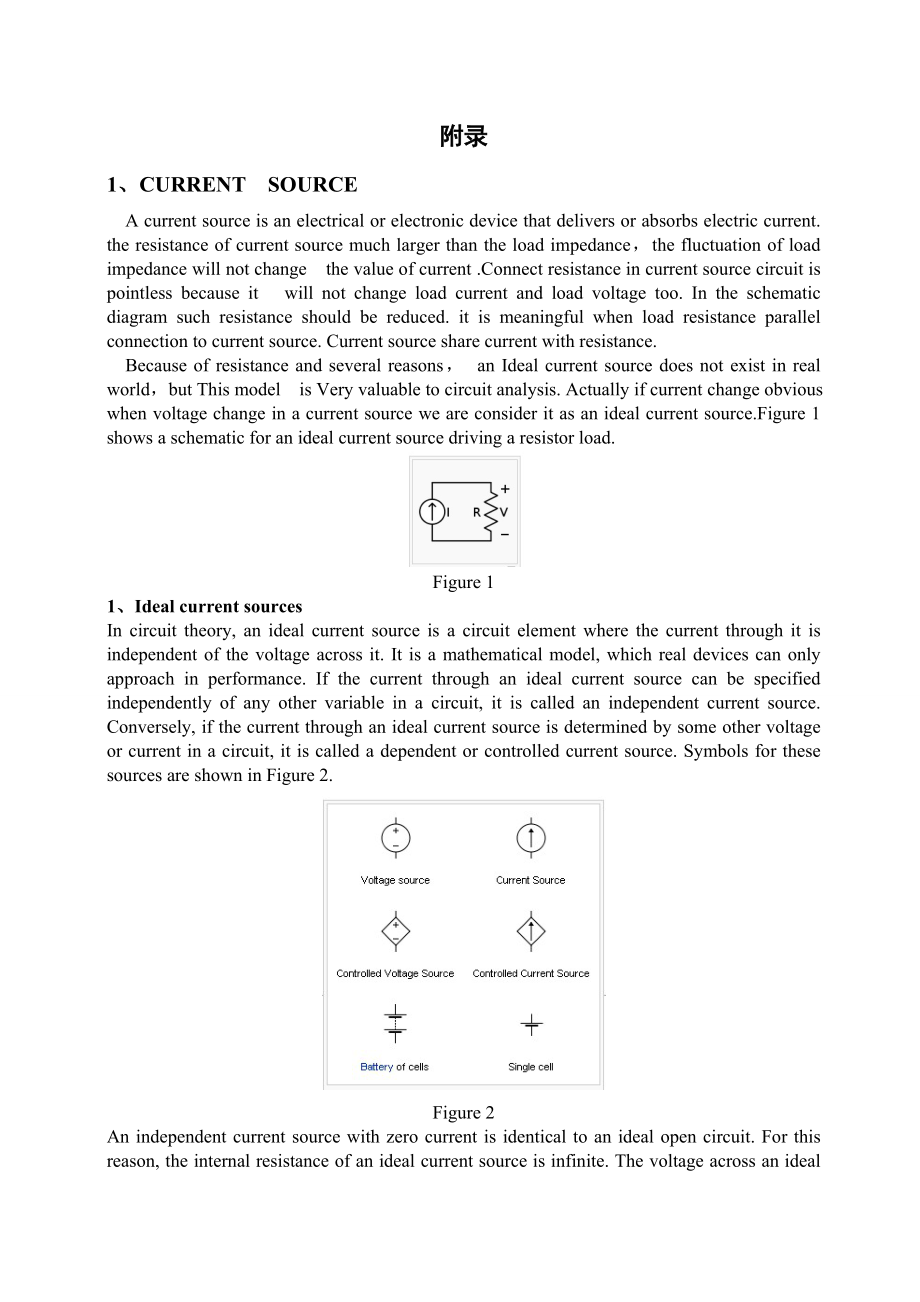
3、ns, an Ideal current source does not exist in real world,but This model is Very valuable to circuit analysis. Actually if current change obvious when voltage change in a current source we are consider it as an ideal current source.Figure 1 shows a schematic for an ideal current source driving a resi
4、stor load.Figure 11、Ideal current sourcesIn circuit theory, an ideal current source is a circuit element where the current through it is independent of the voltage across it. It is a mathematical model, which real devices can only approach in performance. If the current through an ideal current sour
5、ce can be specified independently of any other variable in a circuit, it is called an independent current source. Conversely, if the current through an ideal current source is determined by some other voltage or current in a circuit, it is called a dependent or controlled current source. Symbols for
6、 these sources are shown in Figure 2.Figure 2An independent current source with zero current is identical to an ideal open circuit. For this reason, the internal resistance of an ideal current source is infinite. The voltage across an ideal current source is completely determined by the circuit it i
7、s connected to. When connected to a short circuit, there is zero voltage and thus zero power delivered. When connected to a load resistance, the voltage across the source approaches infinity as the load resistance approaches infinity (an open circuit). Thus, an ideal current source could supply unli
8、mited power forever and so would represent an unlimited source of energy. Connecting an ideal open circuit to an ideal non-zero current source is not valid in circuit analysis as the circuit equation would be paradoxical, e.g., 5 = 0.No real current source is ideal (no unlimited energy sources exist
9、) and all have a finite internal resistance (none can supply unlimited voltage). However, the internal resistance of a physical current source is effectively modeled in circuit analysis by combining a non-zero resistance in parallel with an ideal current source (the Norton equivalent circuit).2、Resi
10、stor current sourceThe simplest current source consists of a voltage source in series with a resistor. The current available from such a source is given by the ratio of the voltage across the voltage source to the resistance of the resistor. For a nearly ideal current source, the value of this resis
11、tor should be very large but this implies that, for a specified current, the voltage source must be very large. Thus, efficiency is low (due to power loss in the resistor) and it is usually impractical to construct a good current source this way. Nonetheless, it is often the case that such a circuit
12、 will provide adequate performance when the specified current and load resistance are small. For example, a 5V voltage source in series with a 4.7k ohms resistor will provide an approximately constant current of 1mA (5%) to a load resistance in the range of 50 to 450 ohms.3、Active current sources Ac
13、tive current sources have many important applications in electronic circuits. Current sources (current-stable resistors) are often used in place of ohmic resistors in analog integrated circuits to generate a current without causing attenuation at a point in the signal path to which the current sourc
14、e is attached. The collector of a bipolar transistor, the drain of a field effect transistor, or the plate of a vacuum tube naturally behave as current sources (or sinks) when properly connected to an external source of energy (such as a power supply) because the output impedance of these devices is
15、 naturally high when used in the current source configuration.4、JFET and N-FET current sourceA JFET can be made to act as a current source by tying its gate to its source. The current then flowing is the IDSS of the FET. These can be purchased with this connection already made and in this case the d
16、evices are called current regulator diodes or constant current diodes or current limiting diodes (CLD). An enhancement mode N channel MOSFET can be used in the circuits listed below.5、Simple transistor current sourceFigure 3 shows a typical constant current source (CCS). DZ1 is a zener diode which,
17、when reverse biased (as shown in the circuit) has a constant voltage drop across it irrespective of the current flowing through it. Thus, as long as the zener current (IZ) is above a certain level (called holding current), the voltage across the zener diode (VZ) will be constant. Resistor R1 supplie
18、s the zener current and the base current (IB) of NPN transistor (Q1). The constant zener voltage is applied across the base of Q1 and emitter resistor R2. The operation of the circuit is as follows:Voltage across R2 (VR2) is given by VZ - VBE, where VBE is the base-emitter drop of Q1. The emitter cu
19、rrent of Q1 which is also the current through R2 is given by.Figure 3Since VZ is constant and VBE is also (approximately) constant for a given temperature, it follows that VR2 is constant and hence IE is also constant. Due to transistor action, emitter current IE is very nearly equal to the collecto
20、r current IC of the transistor (which in turn, is the current through the load). Thus, the load current is constant (neglecting the output resistance of the transistor due to the Early effect) and the circuit operates as a constant current source. As long as the temperature remains constant (or does
21、nt vary much), the load current will be independent of the supply voltage, R1 and the transistors gain. R2 allows the load current to be set at any desirable value and is calculated by or , since VBE is typically 0.65 V for a silicon device. (IR2 is also the emitter current and is assumed to be the
22、same as the collector or required load current, provided hFE is sufficiently large). Resistance R1 at resistor R1 is calculated as,where, K = 1.2 to 2 (so that R1 is low enough to ensure adequate IB), ,and hFE(min) is the lowest acceptable current gain for the particular transistor type being used.A
23、 more common current source in integrated circuits is the current mirror.6、Simple transistor current source with diode compensationTemperature changes will change the output current delivered by the circuit of Figure 3 because VBE is sensitive to temperature. Temperature dependence can be compensate
24、d using the circuit of Figure 4 that includes a standard diode D (of the same semiconductor material as the transistor) in series with the Zener diode as shown in the image on the left. The diode drop (VD) tracks the VBE changes due to temperature and thus significantly counteracts temperature depen
25、dence of the CCS.Resistance R2 is now calculated asSince VD = VBE = 0.65 V,Therefore, .Figure 4This method is most effective for Zener diodes rated at 5.6 V or more. For breakdown diodes of less than 5.6 V, the compensating diode is usually not required because the breakdown mechanism is not as temp
26、erature dependent as it is in breakdown diodes above this voltage.7、Simple transistor current source with LEDAnother method is to replace the Zener diode with a light-emitting diode LED1 as shown in Figure 5. The LED voltage drop (VD) is now used to derive the constant voltage and also has the addit
27、ional advantage of tracking (compensating) VBE changes due to temperature. R2 is calculated as ,and R1 as , where ID is the LED current. Figure 5 Figure 6Another common method is to use feedback to set the current and remove the dependence on the Vbe of the transistor. Figure 6 shows a very common a
28、pproach using an op amp with the non-inverting input connected to a voltage source (such as the Zener in an above example) and the inverting input connected to the same node as the resistor and emitter of the transistor. This way the generated voltage is across the resistor, rather than both the res
29、istor and transistor. (For details, see the article on the ideal op amp - the nullor.) The article on current mirror discusses another example of these so-called gain-boosted current mirrors.8、Other practical sourcesIn the case of opamp circuits sometimes it is desired to inject a precisely known cu
30、rrent to the inverting input (as an offset of signal input for instance) and a resistor connected between the source voltage and the inverting input will approximate an ideal current source with value V/R.9、Inductor type current sourceAmongst other applications, the circuit of Figure 7 using the LM3
31、17 voltage regulator is used to present a source of constant current in Class E (switching) electronic amplifiers.Figure 710、Current and voltage source comparisonMost sources of electrical energy (mains electricity, a battery, .) are best modeled as voltage sources. Such sources provide constant vol
32、tage, which means that as long as the amount of current drawn from the source is within the sources capabilities, its output voltage stays constant. An ideal voltage source provides no energy when it is loaded by an open circuit (i.e. an infinite impedance), but approaches infinite power and current
33、 when the load resistance approaches zero (a short circuit). Such a theoretical device would have a zero ohm output impedance in series with the source. A real-world voltage source has a very low, but non-zero output impedance: often much less than 1 ohm.Conversely, a current source provides a const
34、ant current, as long as the load connected to the source terminals has sufficiently low impedance. An ideal current source would provide no energy to a short circuit and approach infinite energy and voltage as the load resistance approaches infinity (an open circuit). An ideal current source has an
35、infinite output impedance in parallel with the source. A real-world current source has a very high, but finite output impedance. In the case of transistor current sources, impedances of a few megohms (at DC) are typical.An ideal current source cannot be connected to an ideal open circuit because thi
36、s would create the paradox of running a constant, non-zero current (from the current source) through an element with a defined zero current (the open circuit). Nor can an ideal voltage source be connected to an ideal short circuit (R=0), since this would result a similar paradox of finite non zero v
37、oltage across an element with defined zero voltage (the short circuit).Because no ideal sources of either variety exist (all real-world examples have finite and non-zero source impedance), any current source can be considered as a voltage source with the same source impedance and vice versa. These c
38、oncepts are dealt with by Nortons and Thvenins theorems.2、电流源电流源是一种电气或电子设备,可提供或吸收电流。电流源的内阻相对负载阻抗很大,负载阻抗波动不会改变电流大小。在电流源回路中串联电阻无意义,因为它不会改变负载的电流,也不会改变负载上的电压。在原理图上这类电阻应简化掉。负载电阻只有并联在电流源上才有意义,与内阻是分流关系。由于内阻等多方面的原因,理想电流源在真实世界是不存在的,但这样一个模型对于电路分析是十分有价值的。实际上,如果一个电流源在电压变化时,电流的波动不明显,我们通常就假定它是一个理想电流源。图1显示了一个理想电流源
39、驱动电阻负载的原理图。图1理想电流源1、理想电流源在电路理论中,理想电流源流过电路元件的电流与其两端的电压无关。这是一个数学模型。如果一个理想的电流源产生的电流可以独立于任何其他变量,它就可以被称为一个独立的电流源。相反,如果通过其他一些电压或电路中的电流来决定一个理想电流源的电流时,它被称为从属或受控制的电流源。这些源符号,如图2所示。图2各种电流源符号一个独立的电流源与零电流电路是相同的理想开路。基于这个原因,一个理想电流源内阻是无限的。一个理想的电流源的电压完全取决于它的连接电路。因此,一个理想的电流源可提供无限的能量,也代表了无限的能源的来源。连接非零电流源的理想开路是无效的,这在电路
40、的方程分析中将是自相矛盾的,例如,5 = 0。没有真正的理想电流源(不存在无限的能源),并且所有电流源的内部电阻都是有限的(没有人能提供无限的电压)。因此,电流源内部电阻建模的电路结构分析等效于理想电流源与非零电阻并联电路(诺顿等效电路)。2、电阻电流源最简单的电流源由一个电阻与一个电压源串联。目前这样的电流源的来源可以是由电压源的两端电压比电阻器的电阻值提供。对于一个几近完美的电流源,这个电阻值应该是非常大的,但是这意味着,为了提供额定电流,电压源必须是非常大的。因此,这样的电源是低效率的(由于功率在电阻上的损耗),做好这样的电流源也是不切实际的。尽管如此,在很多情况下,这种电路将在负载电阻
41、较小和额定电流较小时提供能够达到性能指标的的参数。例如,在50至450欧姆负载电阻范围,与5V的电压源并联将提供一个大约1mA的恒定电流( 5)。3、主动电流源 主动电流源在电子电路中有许多重要的应用。(电流稳定电阻)电流源通常用在模拟集成电路使用欧姆电阻的地方,电流源的连接不会导致在信号路径中的任何一个点的电流衰减。在电流源配置使用时,一个双极晶体管的集电极,一个场效应晶体管,或一个真空管(或汇漏电流源盘)如果能正确连接到外部的能源来源(如电力供应)那么这些设备是高阻抗输出的。 4、结型场效应管和N - FET电流源一款JFET可以被比作为电源的大门,作为电流源的控制器件。目前市场上流通的是
42、基于场效应管的智能决策系统。可以购买这些已经现有设备,并结合电流稳压二极管或恒流二极管或限流二极管(CLD)连接成电流源。一个增强型N沟道MOSFET,可用于许多电路。5、简单晶体管电流源图3显示了一个典型的恒定电流源(CCS)。 DZ1是一个齐纳二极管,像这种反向偏置时(所示电路),不论通过它电流的大小,都会产生一个恒定的电压降。因此,只要齐纳电流(输出型)超过一定水平(这个水平称为维持电流),对面齐纳二极管(VZ)的电压将保持不变。流过电阻R1的电流就是齐纳电流和NPN晶体管(IB)的基极电流(Q1)。齐纳管的恒定电压适用于整个Q1的基极和发射极电阻R2。电路的操作如下:R2的电压(VR2
43、)由下式中VE- VBE给出,VBE是Q1基极和发射极的电压降。Q1的发射极电流,也就是经过R2的电流,由下式给出图3典型恒流源由于VE不变,VBE在某一给定的温度环境下是不变的,可以得出VR2是恒定的,所以IE是恒定的。由于晶体管的作用,发射极电流IE非常接近集成电路晶体管集电极电流(反过来,是当前通过负载)。因此,负载电流为常数(忽略早期晶体管输出电阻的影响)把电路作为一个恒定电流源使用。只要温度保持不变(或变化不大),负载电流将是电源电压和R1的比值,这与晶体管的增益无关。 R2的允许负载电流在任何可取的范围内,并由计算式或计算R2,由于VBE中通常是0.65 V的硅器件(IR2也是发射
44、极电流,并假设作为集电极或负载所需的电流,同时提供的三级管电流放大倍数足够大)。电阻R1阻值的计算公式为,其中,K= 1.2到2(使R1足够低,以确保有足够的基极电流), 是目前使用的特定类型晶体管中可以接受的最低电流增益。当前更常见的集成电路电流源是镜像电流源。6、简单二极管补偿的晶体管电流源温度的变化会改变输出电流:如图3电路所示,因为VBE对温度很敏感。温度补偿的实现可以用图4电路,包括一个标准二极管D(与晶体管的半导体材料相同)和一种齐纳二极管。该二极管压降(VD)随着VBE由温度的变化而变化,从而大大抵消了对CCS的依赖。电阻R2的计算式,由于VDV,因此, ,R1的计算方法 图4补
45、偿电路。对于小于5.6 V时,该补偿二极管通常不是必需的,因为根据击穿机理它不会像上面那个电压击穿二极管。7、简单晶体管电流源与LED另一种方法是以发光二极管LED1取代齐纳二极管,如图5。 LED的电压降(VD)现在用于推导恒压原理,它有额外的跟踪优势,可用于补偿VBE因温度引起的变化。 R2的计算公式为, R1的计算公式为,其中ID是流过LED的电流。 图5 LED1代替DZ1 图6反馈电路另一种常见的方法是使用反馈来设置电流和消除对晶体管VBE的依赖。图6显示了一个非常普遍的使用方法:把同相输入端连接到一个电压源,反相输入端连接到的电阻和晶体管的发射极相同的节点。这种方式产生的电压在电阻
46、两端,而不是在两个电阻器和晶体管之间。(详细资料,请参阅理想运算放大器的文章 - 零器)有关镜像电流源的文章在讨论另一个所谓镜像电流增益的例子。8、其他实际来源在运算放大电路中,有时候经常需要用到一个已知的精确的反向电流。(作为一个信号,例如输入偏移量)在电压源和反相输入端之间连接一个电阻构成一个电流源,它的值将接近理想值V/R。9、电感式电流源在众多的应用电路中,图7电路采用了LM317稳压器向E类(开关源)电子放大器提供一个恒流源。 图7电感式电流源10、电流源和电压源的比较大部分电能的来源(电力电源,电池,.)都可以作为电压源的最佳模型。这种电源提供恒定的电压,这意味着只要电路从电源吸取
47、的电流在电源的可提供范围内,它的输出电压就保持不变。当电路断开的时候电压源将不提供能量(即电路阻抗无穷大),但是负载电阻趋近于零时(短路)功率和电流趋于无穷大。这种设备的输出阻抗在理论上为零。一个实际的电压源输出阻抗是非常低的,但不为零:通常远小于1欧姆。 同样的道理,电流源提供恒定电流,不管负载是否连接到电流源它的阻抗都是非常低的。一个理想的电流源对短路电路不提供能量,当负载电阻接近无穷大时(开路)它提供的功率和电压都趋于无穷大。一个理想的电流源具有与电源相匹配的无穷大的输出阻抗。一个实际的电流源具有非常高,但有限的输出阻抗。在晶体管电流源例子中,数兆欧阻抗(在直流电路中)是常见的。一个理想电流源不能被连接到一个理想的开路,因为这会形成一个正在运行的非零电流常量(从电流源)通过这与定义零电流(短路)是互相矛盾的。也不能把一个理想电压源连接到一个理想的短路电路(R = 0),因为这将同样会导致一个零电压与非零有限电压的矛盾(短路)。 由于没有任何理想的电源存在(所有现实世界的例子都存在有限的非零电源阻抗),任何电流源都可以看被作为具有相同源阻抗的电压源,反之亦然。这些概念,都是由诺顿和戴维南定理得到的。
- 温馨提示:
1: 本站所有资源如无特殊说明,都需要本地电脑安装OFFICE2007和PDF阅读器。图纸软件为CAD,CAXA,PROE,UG,SolidWorks等.压缩文件请下载最新的WinRAR软件解压。
2: 本站的文档不包含任何第三方提供的附件图纸等,如果需要附件,请联系上传者。文件的所有权益归上传用户所有。
3.本站RAR压缩包中若带图纸,网页内容里面会有图纸预览,若没有图纸预览就没有图纸。
4. 未经权益所有人同意不得将文件中的内容挪作商业或盈利用途。
5. 装配图网仅提供信息存储空间,仅对用户上传内容的表现方式做保护处理,对用户上传分享的文档内容本身不做任何修改或编辑,并不能对任何下载内容负责。
6. 下载文件中如有侵权或不适当内容,请与我们联系,我们立即纠正。
7. 本站不保证下载资源的准确性、安全性和完整性, 同时也不承担用户因使用这些下载资源对自己和他人造成任何形式的伤害或损失。
