 外文翻译基于单片机的多点温度检测系统的设计单片机

《外文翻译基于单片机的多点温度检测系统的设计单片机》由会员分享,可在线阅读,更多相关《外文翻译基于单片机的多点温度检测系统的设计单片机(20页珍藏版)》请在装配图网上搜索。
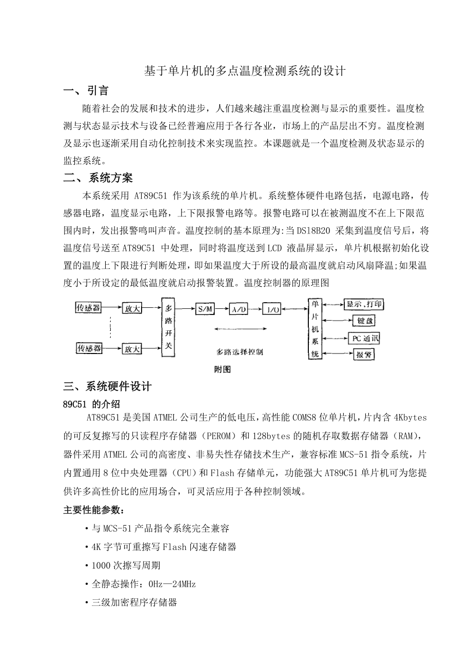
1、基于单片机的多点温度检测系统的设计一、引言随着社会的发展和技术的进步,人们越来越注重温度检测与显示的重要性。温度检测与状态显示技术与设备已经普遍应用于各行各业,市场上的产品层出不穷。温度检测及显示也逐渐采用自动化控制技术来实现监控。本课题就是一个温度检测及状态显示的监控系统。二、系统方案本系统采用 AT89C51 作为该系统的单片机。系统整体硬件电路包括,电源电路,传感器电路,温度显示电路,上下限报警电路等。报警电路可以在被测温度不在上下限范围内时,发出报警鸣叫声音。温度控制的基本原理为:当DSl8B20 采集到温度信号后,将温度信号送至AT89C51 中处理,同时将温度送到LCD 液晶屏显示
2、,单片机根据初始化设置的温度上下限进行判断处理,即如果温度大于所设的最高温度就启动风扇降温;如果温度小于所设定的最低温度就启动报警装置。温度控制器的原理图三、系统硬件设计89C51 的介绍AT89C51是美国ATMEL公司生产的低电压,高性能COMS8位单片机,片内含4Kbytes的可反复擦写的只读程序存储器(PEROM)和128bytes的随机存取数据存储器(RAM),器件采用ATMEL公司的高密度、非易失性存储技术生产,兼容标准MCS-51指令系统,片内置通用8位中央处理器(CPU)和Flash存储单元,功能强大AT89C51单片机可为您提供许多高性价比的应用场合,可灵活应用于各种控制领域
3、。主要性能参数:与MCS-51产品指令系统完全兼容4K字节可重擦写Flash闪速存储器1000次擦写周期全静态操作:0Hz24MHz三级加密程序存储器1288字节内部RAM32个可编程I/O口线2个16位定时/计数器6个中断源可编程串行UART通道低功耗空闲和掉电模式功能特性概述: AT89C51提供以下标准功能:4K字节Flash闪速存储器,128字节内部RAM,32个I/O口线,两个16位定时/计数器,一个5向量两级中断结构,一个全双工串行通信口,片内振荡器及时钟电路。同时,AT89C51可降至0Hz的静态逻辑操作,并支持两种软件可选的节电工作模式。空闲方式停止CPU的工作,但允许RAM,
4、定时/计数器。串行通信口及中断系统继续工作。掉电方式保存RAM中的内容,但振荡器停止工作并禁止其它所有部件工作直到下一个硬件复位。引脚功能说明:VCC:电源电压GND:地P0口:P0口是一组8位漏极开路型双向I/O口,也即地址/数据总线复用口。作为输出口用时,每位能吸收电流的方式驱动8个TTL逻辑门电路,对端口写“1”可作为高阻抗输入端用。在访问外部数据存储器或程序存储器时,这组口线分时转换地址(低8位)和数据总线复用,在访问期间即或内部上拉电阻。在Flash编程时,P0口接收指令字节,而在程序校验时,输出指令字节,校验时,要求外接上拉电阻。P1口:P1是一个带有内部上拉电阻的8位双向I/O口
5、,P1的输出缓冲级可驱动(吸收或输出电流)4个TTL逻辑门电路。对端口写“1”,通过内部的上拉电阻把端口拉到高电平,此时可作输入口。作输入口使用时,因为内部存在上拉电阻,某个引脚被外部信号拉低时会输出一个电流(IIL)。Flash编程和程序校验期间,P1接收低8位地址。P2口:P2是一个带有内部上拉电阻的8位双向I/O口,P2的输出缓冲级可驱动(吸收或输出电流)4个TTL逻辑门电路。对端口写“1”,通过内部的上拉电阻把端口拉到高电平,此时可作输入口。作输入口使用时,因为内部存在上拉电阻,某个引脚被外部信号拉低时会输出一个电流(IIL)。在访问外部程序存储器或16位地址的外部数据存储器(例如执行
6、MOVXDPTR指令)时,P2口送出高8位地址数据。在访问8位地址的外部数据存储器(如执行MOVXRI指令)时,P2口线上的内容在整个访问期间不改变。Flash编程或检验时,P2亦接收高位地址和其它控制信号。P3口:P3口是一组带有内部上拉电阻的8位双向I/O口。P3口输出缓冲级可驱动(吸收或输出电流)4个TTL逻辑门电路。对P3口写入“1”时,它们被内部上拉电阻拉高并可作为输入端口。作输入端时,被外部拉低的P3口将用上拉电阻输出电流(IIL)。P3口还接收一些用于Flash闪速存储器编程和程序校验的控制信号。RET:复位输入。当振荡器工作时,RET引脚出现两个机器周期以上高电平将使单片机复位
7、。ALE/:当访问外部程序存储器或数据存储器时,ALE(地址锁存允许)输出脉冲用于锁存地址的低8位字节。对Flash存储器编程期间,该引脚还用于输入编程脉冲()。即使不访问外部存储器,ALE仍以时钟振荡频率的1/6输出固定的正脉冲信号,因此它可对外输出时钟或用于定时目的。要注意的是:每当访问外部数据存储器时将跳过一个ALE脉冲。如有必要,可通过对特殊功能寄存器(SFR)区中的8EH单元的D0位置位,可禁止ALE操作。该位置位后,只有一条MOVX和MOVC指令ALE才会被激活。此外,该引脚会被微弱拉高,单片机执行外部程序时,应设置ALE无效。:程序储存允许()输出是外部程序存储器的读选通信号,当
8、AT89C51由外部程序存储器取指令(或数据)时,每个机器周期两次有效,即输出两个脉冲。在此期间,当访问外部数据存储器,这两次有效的信号不出现。EA/VPP:外部访问允许。欲使CPU仅访问外部程序存储器(地址为0000HFFFFH),EA端必须保持低电平(接地)。需注意的是:如果加密位LB1被编程,复位时内部会锁存EA端状态。如EA端为高电平(接VCC端),CPU则执行内部程序存储器中的指令。Flash存储器编程时,该引脚加上+12V的编程允许电源VPP,当然这必须是该器件是使用12V编程电压VPP。XTAL1:振荡器反相放大器及内部时钟发生器的输入端。XTAL2:振荡器反相放大器的输出端。R
9、eady/:字节编程的进度可通过RDY/输出信号监测,编程期间,ALE变为高电平“H”后P3.4(RDY/)端电平被拉低,表示正在编程状态(忙状态)。编程完成后,P3.4变为高电平表示准备就绪状态。时钟振荡器:AT89C51中有一个用于构成内部振荡器的高增益反相放大器,引脚XTAL1和XTAL2分别是该放大器的输入端和输出端。这个放大器与作为反馈元件的片外石英晶体 或陶瓷谐振器一起构成自激振荡器。用户也可以采用外部时钟。这种情况下,外部时钟脉冲接到XTAL1端,即内部时钟发生器的输入端,XTAL2则悬空。由于外部时钟信号是通过一个2分频触发器后作为内部时钟信号的,所以对外部时钟信号的占空比没有
10、特殊要求,但最小高电平持续时间和最大的低电平持续时间应符合产品技术条件的要求。空闲节电模式:在空闲工作模式状态,CPU保持睡眠状态而所有片内的外设仍保持激活状态,这种方式由软件产生。此时,片内RAM和所有特殊功能寄存器的内容保持不变。空闲模式可由任何允许的中断请求或硬件复位终止。通过硬件复位也可将空闲工作模式终止。需要注意的是:当由硬件复位来终止空闲工作模式时,CPU通常是从激活空闲模式那条指令的下一条指令开始继续执行程序的,要完成内部复位操作,硬件复位脉冲要保持两个机器周期有效,在这种情况下,内部禁止CPU访问片内RAM,而允许访问其它端口。为了避免可能对端口产生意外写入,激活空闲模式的那条
11、指令后一条指令不应是一条对端口或外部存储器的写入指令。掉电模式:在掉电模式下,振荡器停止工作,进入掉电模式的指令是最后一条被执行的指令,片内RAM和特殊功能寄存器的内容在终止掉电模式前被冻结。退出掉电模式的唯一方法是硬件复位,复位后将重新定义全部特殊功能寄存器但不改变RAM中的内容,在VCC恢复到正常工作电平前,复位应无效,且必须保持一定时间以使振荡器重启动并稳定工作。程序存储器的加密:当加密位LB1被编程时,在复位期间,EA端的逻辑电平被采样并锁存,如果单片机上电后一直没有复位,则锁存起的初始值是一个随机数,且这个随机数会一直保存到真正复位为止。为使单片机能正常工作,被锁存的EA电平值必须与
12、该引脚当前的逻辑电平一致。此外,加密位只能通过整片擦除的方法清除。Flash闪速存储器的编程:AT89C51单片机内部有4K字节的Flash PEROM,这个Flash存储阵列出厂时已处于擦除状态(即所有存储单元的内容均为FFH),用户随时可对其进行编程。编程接口可接收高电压(+12V)或低电压(VCC)的允许编程信号。低电压编程模式适合于用户在线编程系统,而高电压编程模式可与通用EPROM编程器兼容。AT89C51的程序存储器阵列是采用字节写入方式编程的,每次写入一个字节,要对整个芯片内的PEROM程序存储器写入一个非空字节,必须使用片擦除的方式将整个存储器的内容清除。编程方法:编程前,须根
13、据表设置好地址、数据及控制信号。AT89C51编程方法如下: 1、在地址线上加上要编程单元的地址信号。2、在数据线上加上要写入的数据字节。3、激活相应的控制信号。4、在高电压编程方式时,将EA/VPP端加上+12V编程电压。5、每对Flash存储阵列写入一个字节或每写入一个程序加密位,加上一个ALE/编程脉冲。改变编程单元的地址和写入的数据,重复15步骤,直到全部文件编程结束。每个字节写入周期是自身定时的,通常约为1.5ms。数据查询:AT89C51单片机用数据查询方式来检测一个写周期是否结束,在一个写周期中,如需读取最后写入的那个字节,则读出的数据最高位是原来写入字节最高位的反码。写周期完成
14、后,有效的数据就会出现在所有输出端上,此时,可进入下一个字节的写周期,写周期开始后,可在任意时刻进行数据查询。程序校验:如果加密位LB1、LB2没有进行编程,则代码数据可通过地址和数据线读回原编写的数据。加密位不可直接校验,加密位的校验可通过对存储器的校验和写入状态来验证。芯片擦除:利用控制信号的正确组合并保持ALE/引脚10ms的低电平脉冲宽度即可将PEROM阵列(4K字节)和三个加密位整片擦除,代码陈列在片擦除操作中将任何非空单元写入“1”,这步骤需再编程之前进行。读片内签名字节:读签名字节的过程和单元030H、031H及032H的正常校验相仿,只需将P3.6和P3.7保持低电平,返回值意
15、义如下:(030H)=1EH声明产品由ATMEL公司制造(031H)=51H声明为AT89C51单片机(032H)=FFH声明为12V编程电压(032H)=05H声明为5V编程电压编程接口:采用控制信号的正确组合可对Flash闪速存储阵列中的每一代码字节进行写入和存储器的整片擦除,写操作周期是自身定时的,初始化后它将自动定时到操作完成。2.DS18B20 传感器的介绍在传统的模拟信号远距离温度测量系统中,需要很好的解决引线误差补偿问题、多点测量切换误差问题和放大电路零点漂移误差问题等技术问题,才能够达到较高的测量精度。另外一般监控现场的电磁环境都非常恶劣,各种干扰信号较强,模拟温度信号容易受到
16、干扰而产生测量误差,影响测量精度5。因此,在温度测量系统中,采用抗干扰能力强的新型数字温度传感器是解决这些问题的最有效方案, 与其它温度传感器相比DSl820 具有以下特点:(1)独特的单线接口方式。DSl820 在与微处理器连接时仅需要一条接口线即可实现微处理器与DSl820 的双向通讯。(2)多点功能简化了分布式温度检测的应用。(3)DSl820 在使用中无需任何外围元件。(4)可用数据线供电,电压范围从3.0V 到5.5V。(5)可测量的温度范围从-55到+125,增量值0. 5;华氏温度范围从-67 到+257,增量值09。(6)支持多点组网功能。多个DS1820 可以并接在同一条总线
17、上,实现多点测温。(7)9 位的温度分辨率。测量结果以9 位数字量方式串行传送。(8)用户可设定温度报警门限值。(9)有超温度搜寻功能。(1) DSl8B20 的工作原理DS18B20 的内部结构DSl8B20 的测温原理框图如图3.2 所示。图中低温度系数品振的振荡频率受温度影响很小,用于产生同定频率的脉冲信号送给计数器l。高温度系数晶振随温度变化其振荡频率明显改变。所产生的信号作为计数器2 的脉冲输入。计数器1、计数器2 和温度寄存器被预置在-55所对应的一个基数值。计数器l 对低温度系数晶振产生的脉冲信号进行减法计数,当计数器1 的预置值减到O 时,温度计数器的值将加l,计数器l 的预置
18、值将被重新装人,计数器l 重新开始对低温度系数晶振产生的脉冲信号进行计数,如此循环直到计数器2 计数到O 时,停止温度寄存器的累加,此时温度寄存器中的数值即为所测温度。图3.2 中的斜率累加器用于补偿和修正测温过程中的非线性,其输出小于修正计数器l 的预置值。(2) DS18B20 与AT89C51 的接口方式DS18B20 与单片机的连接方式有两种:即寄生电源方式和外部电源方式。寄生电源方式:在寄生电源供电方式下,DS18B20 从单线信号线上汲取能量:在信号线DQ 处于高电平期间把能量储存在内部电容里,在信号线处于低电平期间消耗电容上的电能工作,直到高电平到来再给寄生电源(电容)充电。寄生
19、电源方式有三个好处: 1)进行远距离测温时,无需本地电源。 2)可以在没有常规电源的条件下读取ROM。 3)电路更加简洁,仅用一根I/O 口实现测温。要想使DS18B20 进行精确的温度转换,I/O 线必须保证在温度转换期间提供足够的能量,由于每个DS18B20 在温度转换期间工作电流达到1mA,当几个温度传感器挂在同一根I/O 线上进行多点测温时,只靠4.7K 上拉电阻就无法提供足够的能量,会造成无法转换温度或温度误差极大。外部电源供电方式:在外部电源供电方式下,DS18B20 工作电源由VDD 引脚接入,此时I/O 线不需要强上拉,不存在电源电流不足的问题,可以保证转换精度,同时在总线上理
20、论可以挂接任意多个DS18B20 传感器,组成多点测温系统。本系统采用外部电源方式。连接方法即DS18B20 的1 脚接地,2 脚(DQ 引脚)与AT89C51 的一根I/O 口线相连,3 脚接+5V。在A89S52 的I/O 口线与+5V 之间连接一4.7K 的上拉电阻,以保证数据采集的正常进行。若要组成多点温度检测系统,可在单片机的同一根I/O 口线上,以相同的连接方法并联多片DS18B20 芯片。3、LCD1602 液晶屏1602 液晶显示模块可以和单片机AT89C51 直接接口。 4、蜂鸣器驱动电路由于蜂鸣器的工作电流一般比较大,以致于单片机的I/O 口是无法直接驱动的,所以要利用放大
21、电路来驱动,一般使用三极管来放大电流就可以了。当所测的温度低于6 摄氏度时,报警。5、风扇电路当所测的温度高于80 摄氏度时,启动风扇电路。因为工作电流比较大,所以用放大电路来驱动,即用三极管来放大电流就可以了。当温度高于80时,给单片机一个命令,单片机P26 引脚输出高电平,三极管导通,风扇电路接通,电风扇开始转动,从而起到降温作用。四、系统的软件设计本系统采用AT89C51 作为核心处理器件,把经过DSl8B20 现场实时采集到的温度数据,存入AT89C51 的内部数据存储器,送液晶显示,并与预先设定值进行比较,然后由单片机输出信号去控制风扇电路和报警电路。多功能温度检测显示系统软件主要包
22、括:函数声明、延迟时间函数、DS18B20 初始化函数、读出DS18B20 当前的温度、温度数据转化成液晶字符显示等程序。五、小结随着工业的不断发展,对温度测量的要求来越高,而且测量范围也越来越广,因此对温度检测技术的要求也越来越高。本文介绍了以DSl8B20 新型数字温度传感器、AT89C51 单片机、LCD1602 液晶显示模块为主体构建的温度检测显示系统。说明了系统硬件电路、系统主程序与各模块子程序的设计。本系统采用的是DALLAS 公司推出的数字式温度传感器DS18B20,无需外加AD 即可输出数字量,把温度信号直接转换成串行数字信号供微机处理。因此。该系统具有硬件电路结构简单、转换精
23、度高、显示结果清晰稳定、成本低等显着优点。在诸如粮库测温、智能建筑、中央空调等多种需要温度检测的场合具有较好的应用前景。 本文摘译自:atmel -AT89C51中文资料DATSHEET 规格书 DS18B20的英文数据手册 DS18B20 Programmable Resolution 1-Wire Digital ThermometerBased on SCM multi-functional temperature testing system design1、prefaceWith the development of society and the technological pro
24、gress, people pay more and more attention to the importance of temperature detection and display. Temperature detection and status display technology and equipment has been widely applied in industries, products on the market emerge in endlessly. Temperature testing and also gradually adopt the auto
25、matic control technology to realize the monitor. This topic is a temperature testing and status of the monitoring system.2、System solutionsThis system USES the monolithic integrated circuit AT89C51 as this system. The whole system, the hardware circuit including power supply circuit, sensor, the tem
26、perature display circuit circuit, upper alarm circuit . The alarming circuit can be measured in upper temperature range, screaming voice alarm. The basic principle for the temperature control DSl8B20: when the temperature signal acquisition to after temperature signal sent to handle, AT89C51 tempera
27、ture to LCD screen, SCM according to initialize the upper temperature setting, namely, if the judgement of temperature than the highest temperature cooling fan is started, If the temperature is less than the lowest temperature setting on alarm device. 3、The system hardware design(1)AT89C51 SCM are i
28、ntroducedThe AT89C51 is a low-power, high-performance CMOS 8-bit microcomputer with 4K bytes of Flash programmable and erasable read only memory (PEROM) and 128 bytes of data random-access memory(RAM). The device is manufactured using ATMEL Co.s high-density nonvolatile memory technology and is comp
29、atible with the industry-standard MCS-51 instruction set and pin-out. The on-chip Flash allows the program memory to be reprogrammed in-system or by a conventional nonvolatile memory programmer. By combining a versatile 8-bit CPU with Flash on a monolithic chip, the ATMEL Co.s AT89C51 is a powerful
30、microcomputer which provides a highly-flexible and cost-effective solution to many embedded control applications.Features:Compatible with instruction set of MCS-51 products4K bytes of in-system reprogrammable Flash memoryEndurance: 1000 write/erase cyclesFully static operation: 0 Hz to 24 MHzThree-l
31、evel program memory lock1288-bit internal RAM32 programmable I/O linesTwo 16-bit Timer/CountersSix interrupt sourceProgrammable serial channelLow-power idle and Power-down modesFunction Characteristic Description:The AT89C51 provides the following standard features: 4K bytes of Flash memory, 128 byt
32、es of RAM, 32 I/O lines, two 16-bit timer/counters, a five vector two-level interrupt architecture, a full duplex serial port, on-chip oscillator and clock circuitry. In addition, the AT89C51 is designed with static logic for operation down to zero frequency and supports two software selectable powe
33、r saving modes. The Idle Mode stops the CPU while allowing the RAM, timer/counters, serial port and interrupt system to continue functioning. The Power-down Mode saves the RAM contents but freezes the oscillator disabling all other chip functions until the next hardware reset.Pin Description:VCC: Su
34、pply voltageGND: GroundPort 0: Port 0 is an 8-bit open-drain bi-directional I/O port. As an output port, each pin can sink eight TTL inputs. When 1s are written to port 0 pins, the pins can be used as high impedance inputs.Port 0 may also be configured to be the multiplexed low order address/bus dur
35、ing accesses to external program and data memory. In this mode P0 has internal pull ups. Port 0 also receives the code bytes during Flash programming, and outputs the code bytes during program verification. External pull ups are required during program verification.Port 1: Port 1 is an 8-bit bidirec
36、tional I/O port with internal pull ups. The Port 1 output buffers can sink/source four TTL inputs. When 1s are written to Port 1 pins they are pulled high by the internal pull ups and can be used as inputs. As inputs, Port 1 pins that are externally being pulled low will source current (IIL) because
37、 of the internal pull ups. Port 1 also receives the low-order address bytes during Flash programming and verification.Port 2: Port 2 is an 8-bit bi-directional I/O port with internal pull ups. The Port 2 output buffers can sink/source four TTL inputs. When 1s are written to Port 2 pins they are pull
38、ed high by the internal pull ups and can be used as inputs. As inputs, Port 2 pins that are externally being pulled low will source current (IIL) because of the internal pull ups.Port 2 emits the high-order address byte during fetches from external program memory and during accesses to external data
39、 memory which uses 16-bit addresses (MOVX DPTR). In this application, it uses strong internal pull ups when emitting 1s. During accesses to external data memory which uses 8-bit addresses (MOVX RI). Port 2 emits the contents of the P2 Special Function Register.Port 2 also receives the high-order add
40、ress bits and some control signals during Flash programming and verification.Port 3: Port 3 is an 8-bit bi-directional I/O port with internal pull ups. The Port 3 output buffers can sink/source four TTL inputs. When 1s are written to Port 3 pins they are pulled high by the internal pull ups and can
41、be used as inputs. As inputs, Port 3 pins that are externally being pulled low will source current (IIL) because of the pull ups.Port 3 also receives some control signals for Flash programming and verification.RST: Reset input. A high on this pin for two machine cycles while the oscillator is runnin
42、g resets the device.ALE/: Address Latch Enable output pulse for latching the low byte of the address during accesses to external memory. This pin is also the program pulse input () during Flash programming. In normal operation ALE is emitted at a constant rate of 1/6 the oscillator frequency, and ma
43、y be used for external timing or clocking purposes. Note, however, that one ALE pulse is skipped during each access to external Data Memory. If desired, ALE operation can be disabled by setting bit 0 of SFR location 8EH. With the bit set, ALE is active only during a MOVX or MOVC instruction. Otherwi
44、se, the pin is weakly pulled high. Setting the ALE-disable bit has no effect if the microcontroller is in external execution mode.:Program Store Enable is the read strobe to external program memory. When the AT89C51 is executing code from external program memory, is activated twice each machine cycl
45、e, except that two activations are skipped during each access to external data memory.EA/VPP:External Access Enable. EA must be strapped to GND in order to enable the device to fetch code from external program memory locations starting at 0000H up to FFFFH. Note, however, that if lock bit 1 is progr
46、ammed, EA will be internally latched on reset. EA should be strapped to VCC for internal program executions. This pin also receives the 12-volt programming enable voltage (VPP) during Flash programming, for parts that require 12-volt VPP.XTAL1:Input to the inverting oscillator amplifier and input to
47、 the internal clock operating circuit.XTAL2:Output from the inverting oscillator amplifier.Ready/: The progress of byte programming can also be monitored by the RDY/output signal. P3.4 is pulled low after ALE goes high during programming to indicate BUSY. P3.4 is pulled high again when programming i
48、s done to indicate READY.Oscillator Characteristics:XTAL1 and XTAL2 are the input and output, respectively, of an inverting amplifier which can be configured for use as an on-chip oscillator. Either a quartz crystal or ceramic resonator may be used. To drive the device from an external clock source,
49、 XTAL2 should be left unconnected while XTAL1 is driven.There are no requirements on the duty cycle of the external clock signal, since the input to the internal clocking circuitry is through a divide by two flip trigger, but minimum and maximum voltage high and low time specifications must be obser
50、ved.Idle Mode:In idle mode, the CPU puts itself to sleep while all the on-chip peripherals remain active. The mode is invoked by software. The content of the on-chip RAM and all the special functions registers remain unchanged during this mode. The idle mode can be terminated by any enabled interrup
51、t or by a hardware reset.It should be noted that when idle is terminated by a hardware reset, the device normally resumes program execution, from where it left off, up to two machine cycles before the internal reset algorithm takes control. On-chip hardware inhibits access to internal RAM in this ev
52、ent, but access to the port pins is not inhibited. To eliminate the possibility of an unexpected write to a port pin when Idle is terminated by reset, the instruction following the one that invokes Idle should not be one that writes to a port pin or to external memory.Power-down Mode:In the power-do
53、wn mode, the oscillator is stopped, and the instruction that invokes power-down is the last instruction executed. The on-chip RAM and special function registers retain their values until the power-down mode is terminated. The only exit from power-down is a hardware reset. Reset redefines the special
54、 function registers but does not change the on-chip RAM. The reset should not be activated before VCC is restored to its normal operating level and must be held active long enough to allow the oscillator to restart and stabilize.Program Memory Lock Bits:When lock bit 1 is programmed, the logic level
55、 at the EA pin is sampled and latched during reset. If the device is powered up without a reset, the latch initializes to a random value, and holds that value until reset is activated. It is necessary that the latched value of EA be in agreement with the current logic level at that pin in order for
56、the device to function properly.Programming the Flash:The AT89C51 is normally shipped with the on-chip Flash memory array in the erased state (that is, contents = FFH) and ready to be programmed. The programming interface accepts either a high-voltage (12-volt) or a low-voltage (VCC) program enable
57、signal. The low-voltage programming mode provides a convenient way to program the AT89C51 inside the users system, while the high-voltage programming mode is compatible with conventional third party Flash or EPROM programmers.The AT89C51 is shipped with either the high-voltage or low-voltage program
58、ming mode enabled. The AT89C51 code memory array is programmed byte-by-byte in either programming mode. To program any nonblank byte in the on-chip Flash memory, the entire memory must be erased using the chip erase mode. Programming Algorithm: Before programming the AT89C51, the address, data and c
59、ontrol signals should be set up according to the Flash programming mode table .To program the AT89C51, take the following steps:1. Input the desired memory location on the address lines.2. Input the appropriate data byte on the data lines.3. Activate the correct combination of control signals.4. Rai
60、se EA/VPP to 12V for the high-voltage programming mode.5. Pulse ALE/once to program a byte in the Flash array or the lock bits. The byte-write cycle is self-timed and typically takes no more than 1.5ms. Repeat steps 1 through 5, changing the address and data for the entire array or until the end of
61、the object file is reached.Data Polling: The AT89C51 features Data Polling to indicate the end of a write cycle. During a write cycle, an attempted read of the last byte written will result in the complement of the written datum on PO.7. Once the write cycle has been completed, true data are valid o
62、n all outputs, and the next cycle may begin. Data polling may begin any time after a write cycle has been initiated.Program Verify: If lock bits LB1 and LB2 have not been programmed, the programmed code data can be read back via the address and data lines for verification. The lock bits cannot be ve
63、rified directly. Verification of the lock bits is achieved by observing that their features are enabled.Chip Erase: The entire Flash array is erased electrically by using the proper combination of control signals and by holding ALE/ low for 10 ms. The code array is written with all “1”s. The chip er
64、ase operation must be executed before the code memory can be re-programmed.Reading the Signature Bytes: The signature bytes are read by the same procedure as a normal verification of locations 030H, 031H, and 032H, except that P3.6 and P3.7 must be pulled to a logic low. The values returned are as follows:(030H) = 1EH indicates manufactured by ATMEL(031H) = 51H indicates AT89C51 single-chip(032H) = FFH indicates 12V programming(032H) = 05H indicates 5V programmingProgramming Interface:Every code byte in th
- 温馨提示:
1: 本站所有资源如无特殊说明,都需要本地电脑安装OFFICE2007和PDF阅读器。图纸软件为CAD,CAXA,PROE,UG,SolidWorks等.压缩文件请下载最新的WinRAR软件解压。
2: 本站的文档不包含任何第三方提供的附件图纸等,如果需要附件,请联系上传者。文件的所有权益归上传用户所有。
3.本站RAR压缩包中若带图纸,网页内容里面会有图纸预览,若没有图纸预览就没有图纸。
4. 未经权益所有人同意不得将文件中的内容挪作商业或盈利用途。
5. 装配图网仅提供信息存储空间,仅对用户上传内容的表现方式做保护处理,对用户上传分享的文档内容本身不做任何修改或编辑,并不能对任何下载内容负责。
6. 下载文件中如有侵权或不适当内容,请与我们联系,我们立即纠正。
7. 本站不保证下载资源的准确性、安全性和完整性, 同时也不承担用户因使用这些下载资源对自己和他人造成任何形式的伤害或损失。
